What is BJT and its Configuration?
BJT Configuration
- A configuration refers to the way three terminals of BJT are used in amplifier.
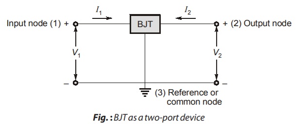
- Based upon the reference or common node a BJT can be used in three configurations as given in Table-3.2.
| S.No. | Configuration | Input node | Output node |
|---|---|---|---|
| 1. | Common Base (CB) | E | C |
| 2. | Common Emitter (CE) | B | C |
| 3. | Common Collector (CC) | B | E |
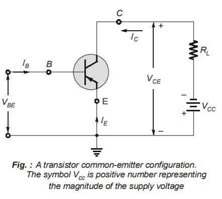
The Common-Emitter Configuration
Most transistor circuits have the emitter terminal common to both input and output. Such a Common-Emitter (CE) or grounded-emitter, configuration is indicated in figure.
In common-emitter configuration, the input current and output voltage are taken as independent variables, whereas the input voltage and output current are the dependent variables.
We may write
Above equation describes the family of input characteristics and the family of output characteristics respectively.
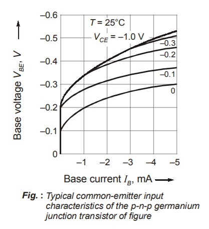
The Input Characteristics
Typical input characteristic curves for a p-n-p junction Germanium transistor are given in figure.
- With collector shorted to the emitter and forward- biased emitter, the input characteristics are essentially that of a forward biased-diode.
- If VBE becomes zero, then IB will be zero, since under these conditions both emitter and collector junctions will be short-circuited.
- For any other value of VCE, base current for V BE= 0 is not actually zero but is too small to be observed in figure.
- In general increase in | VCE | with constant VBE causes a decrease in base width W (the Early effect) and results in decreased recombination base current.
- These considerations account for the shape of input characteristics shown in figure.
The Output Characteristics
Typical output characteristics curves for a p-n-p junction Germanium transistor are given in figure below.
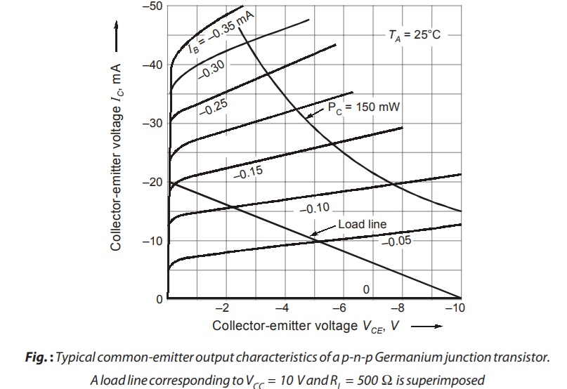
The family of curves may be divided into three regions. These are active region, cut-off region and saturation region.
Active Region
- In above figure, active region is the area to the right of the ordinate VCE = a few tenths of a volt and above IB = 0.
- In this region the transistor output current responds most sensitively to an input signal.
- If transistor is to be used as an amplifying device without appreciable distortion, it must be restricted to operate in this region.
- It should also be clear that a slight change in a has large effect on the common-emitter curves, and hence that common-emitter characteristics are normally subjected to wide variation even among transistor of a given type. This variability is caused by the fact that IB is the difference between large and nearly equal currents, IE and IC.
Cut-off Region
We might be inclined to think that cut-off in figure above occurs at the intersection of the load line with current IB = 0; however we now find that appreciable collector current may exists under these conditions. We have
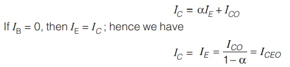
- The actual collector current with collector junction reverse-biased and base open-circuited is designated by the symbol ICEO.
- Since, even in the neighbourhood of cut-off, a may be as large as 9 for Germanium, then IC≃10ICO at zero base current.
- Accordingly, in order to cut-off the transistor, it is not enough to reduce IB to zero. Instead, it is necessary to reverse-bias the emitter junction slightly.
- In summary, cut-off means that IE = 0, IC = I CO, IB = –I C = –ICO, and VBE is a reverse voltage whose magnitude is of the order of 0.1 V for Germanium and 0 V for a Silicon transistor.
Saturation Region
- The saturation region may be defined as the one where collector junction (as well as the emitter junction) is forward-biased.
- In this region bottoming occurs, |VCE| drops to few tenths of a volt, and the collector current is approximately independent of base current, for given values of VCC and RL.
- Hence we may consider that onset of saturation takes place at knee of the transistor curves in figure.
Properties
- Moderate input resistance (around 1 kΩ).
- Moderate output resistance (50 kΩ to 500 kΩ).
- Moderate current gain (Typical value 49).
- Moderate voltage gain.
- Highest power gain (Typical value 4226).
- Output and input voltages are out of phase i.e. phase shift = 180°.
Application
It is the most common and frequently used amplifier circuit.
Dear Aspirants,
Your preparation for GATE, ESE, PSUs, and AE/JE is now smarter than ever — thanks to the MADE EASY YouTube channel.
This is not just a channel, but a complete strategy for success, where you get toppers strategies, PYQ–GTQ discussions, current affairs updates, and important job-related information, all delivered by the country’s best teachers and industry experts.
If you also want to stay one step ahead in the race to success, subscribe to MADE EASY on YouTube and stay connected with us on social media.
MADE EASY — where preparation happens with confidence.
MADE EASY is a well-organized institute, complete in all aspects, and provides quality guidance for both written and personality tests. MADE EASY has produced top-ranked students in ESE, GATE, and various public sector exams. The publishing team regularly writes exam-related blogs based on conversations with the faculty, helping students prepare effectively for their exams.