Silicon Controlled Rectifier (SCR)
- SCR is the oldest and first member of the thyristor family.
- It is called SCR because, silicon is used for its construction and its operation as a rectifier (very low resistance in forward conduction and very high resistance in the reverse direction) can be controlled.
- It has three terminals {see fig. (a)} : (i) Anode (A); (ii) Cathode (K); (iii) Gate (G)
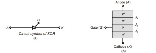
- The structure of SCR {see fig. (b)}
The terminal connected to outer ‘p’ region is called Anode (A).
The terminal connected to outer ‘n’ region is called Cathode (K).
The terminal connected to inner ‘p’ region is called the Gate (G). - SCR is a unidirectional device. It blocks the current flow from cathode to anode.
Static V-I Characteristics of SCR
- An elementary circuit diagram for obtaining static V-I characteristics of SCR is shown in figure,
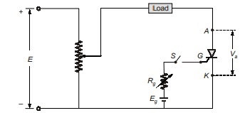
- The Anode and Cathode are connected to main source through the load.
- The Gate and Cathode are fed from another source ‘Eg’.
- The static V-I characteristics of SCR are shown below.
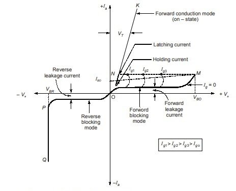
Va = Anode voltage; Ia = Anode current
VBO = Forward breakover voltage
VBR = Reverse breakdown voltage
Ig = Gate current
IL = Latching current
IH = Holding current
- The three basic modes of operation of SCR are :
(i) Forward blocking mode; (ii) Forward conduction mode; (iii) Reverse blocking mode
1. Forward Blocking Mode
- When anode is at a higher potential than cathode, with gate circuit open, thyristor is said to be forward biased.
- It is seen from the figure that J1, J3 are forward bias but junction J2 is reverse bias.
- In this mode, a small current, called forward leakage current flows from anode to cathode.
- OM in the VI characteristics represents the forward blocking mode of SCR.
- SCR is treated as an open switch in the forward blocking mode.
Forward Conduction Mode
- When anode to cathode forward voltage is increased with gate circuit open, reverse biased junction J2 will have an avalanche breakdown at a voltage called forward breakover voltage VBO.
- After this breakdown, thyristor gets turned ON with point ‘M’ at once shifting to ‘N’. Here NK represents the forward conduction mode.
- A thyristor can be brought from forward blocking mode to forward conducting mode by turning it on by applying
(i) a positive Gate pulse between gate and cathode (or)
(ii) a forward breakover voltage (VBO) across anode and cathode - Voltage drop across the SCR ‘VT’ increases slightly with an increase in anode current. It can be seen from NK
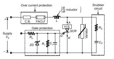
Protection of SCR
di/dt Protection
A thyristor requires a minimum time to spread the current conduction uniformly throughout the junctions. If the rate of rise of anode current is very fast compared with the spreading velocity of a turn ON process, a localized “hot spot” heating may occur due to high current density and the device may fail, as a result of excessive temperature.
The practical devices must be connected against high di/dt. Let us consider the circuit in figure. Under steady state 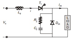 operation, Dm conducts when thyristor T1 is off. If T1is fired when Dm is still conducting, di/dt can be very high and limited only by the stray inductance of the circuit.
The di/dt is limited by adding a series inductor Ls , as shown in figure. The forward di/dt is di/dt = Vs/Ls
dv/dt Protection
- If the rate of rise of suddenly applied voltage across thyristor is high the device may get turned-on. Such phenomena of turning on a thyristor, called dv/dt turn-on must be avoided as it leads to false operation.
- False turn-on of a SCR by large dv/dt, even with out application of gate signal can be prevented by using a Snubber circuit in parallel with the device.
Design of Snubber Circuit
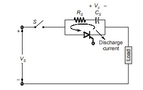
A snubber circuit consists of a series combination of resistance Rs and capacitance Cs in parallel with the thyristor as shown in figure.
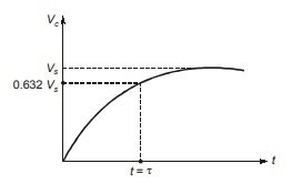
When switch ‘s’ is closed, a sudden voltage is appearing across the circuit. Capacitor Cs behaves like a short circuit, therefore voltage across SCR is zero. With the passage of time, voltage across Cs built up at a slow rate such that the dv/dt across ‘Cs ’ and therefore across SCR is less than the specified maximum dv/dt rating of the device.
In order to limit the magnitude of discharge current, a resistance Rs is inserted in series with ‘Cs’
Over Voltage Protection
A SCR may be subjected to internal or external over voltages.
Internal Over Voltages
Due to the presence of the series inductance Ls of the SCR circuit, large transient voltages ![]() is produced and this internal voltage may be several times the breakover voltage of the SCR, the thyristor may be
is produced and this internal voltage may be several times the breakover voltage of the SCR, the thyristor may be
destroyed permanently.
External Over Voltages
- Over voltages are caused due to the lightning strokes and switching surges.
- For reliable operation, the over voltages must be suppressed by adapting voltage clamping (v.c) device.
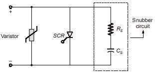
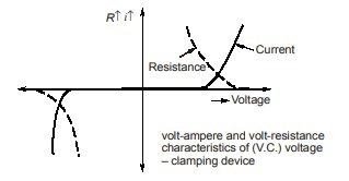
- A voltage clamping (V.C) device is a non-linear resistor connected across SCR as shown in figure. The V.C. device has falling resistance characteristics with increasing voltage. Under normal conditions the device has a high resistance and draws only a small leakage current. When a voltage surge appears, the V.C. device operates in low resistance region and produces a short-circuit across SCR. After the surge is dissipated it returns to normal high resistance.
Over Current Protection
If a SCR is subjected to over current due to faults, short circuits (or) surge currents, its junction temperature may exceed the rated value and the device may be damaged. There is a need for the over current protection of SCR.
- Fast acting current limiting fuse (FACLF)
- Circuit breakers are used
Gate Protection
- Over voltages and over currents across the gate circuit can cause false triggering of the SCR.
- Protection against over voltages is achieved by connecting a zener diode across the gate circuit.
- Protection against the over current is achieved by connecting a resistor ‘R2’ in series with gate circuit.
- A capacitor and a resistor are also connected across gate to cathode to by pass the noise signals.
Circuit Components Showing the Thyristor Protection
Thermal Protection
If temperature increases, insulation is weakened, resulting in leakage currents which interference with the operation. Heat sinks which include aluminium discs are used along with ventilating ducts, increased surface area, coolants are used.
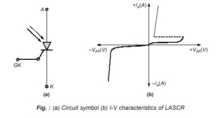
LASCR (Light Activated Thyristor)
- LASCR is turned on by direct radiation of silicon with light.
- The triggering current produced because of the electron-hole pairs which are created due to radiation under the influence of electric field.
- It is used in high-voltage and high-current applications, e.g., in HVDC transmission.
- The typical di/dt rating is 250 A/µs and dv/dt rating could be as high as 2000 V/µs.
The DIAC (Bidirectional Thyristor Diode)
- DIAC stands for Diode for Alternating Current.
- It is a device which has two electrodes and which conducts electrical current only after its breakover voltage (VBO).
- The main application of DIAC is in TRIAC triggering circuit, lamp dimmer circuit, heat control circuit etc.
- If voltage V12, with terminal 1 positive with respect to terminal 2, exceeds breakover voltage VB01, then structure pnpn conducts.
- In case terminals 2 is positive with respect to terminal 1 and when V21 exceeds break over voltage VB02, structure pnpn′ conducts.
- I-V characteristics of a DIAC.
NOTE: The term DIAC is obtained from capital letters, Diode that can work on AC. A DIAC is some times called a gate less TRIAC.
TRIAC
A TRIAC is a bidirectional thyristor with three terminals. It is used extensively for the control of power in ac circuits.
TRIAC is the word derived by combining the capital letters from the word TRIode and AC.
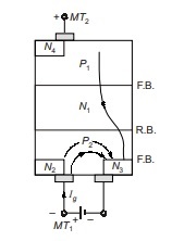
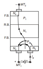
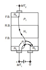
Its three terminals are usually designated as MT1 (Main terminal 1), MT2 and the gate.
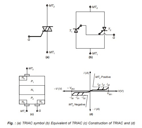
The TRIAC can however be turned on in each half cycle of the applied voltage by applying a positive (or) negative voltage to the gate with respect to terminal MT1.
The turn-on process of a triac can be explained as under:
MT2 positive and Gate current is also positive: When Gate current has injected sufficient charge into P2 layer, reverse biased junction N1P2 breaks down.
As a result, triac starts conducting through P1, N1, P2, N2 layers.
MT2 is positive but Gate is negative: Gate current flows through P2 N3 junction.
Reverse biased junction N1P2 is forward biased by injecting sufficient charge into P2.
As a result, TRIAC starts conducting through P1N1P2N3
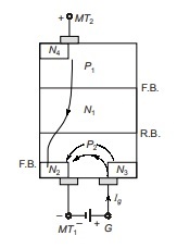
MT2 is negative but Gate current is positive: Gate current Ig forward biases P2N2 junction. Layer N2
injects electrons into P2 layer. As a reset, reverse biased junction N1P1 breaks down.
The path P2N1P1N4 is completely turned-on.
Both MT2 and Gate current are negative:
The gate current Ig flows from P2 to N3.
Reverse biased junction N1P1 is broken, and finally, the path P2 N1 P1 N4 is turned on.
<< Previous | Next >>
Must Read: What is Power Electronics?
Dear Aspirants,
Your preparation for GATE, ESE, PSUs, and AE/JE is now smarter than ever — thanks to the MADE EASY YouTube channel.
This is not just a channel, but a complete strategy for success, where you get toppers strategies, PYQ–GTQ discussions, current affairs updates, and important job-related information, all delivered by the country’s best teachers and industry experts.
If you also want to stay one step ahead in the race to success, subscribe to MADE EASY on YouTube and stay connected with us on social media.
MADE EASY — where preparation happens with confidence.
MADE EASY is a well-organized institute, complete in all aspects, and provides quality guidance for both written and personality tests. MADE EASY has produced top-ranked students in ESE, GATE, and various public sector exams. The publishing team regularly writes exam-related blogs based on conversations with the faculty, helping students prepare effectively for their exams.