MOSFET
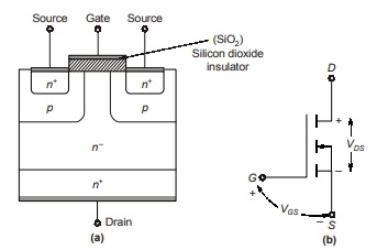
A metal oxide semiconductor field effect transistor (MOSFET) has three terminals called drain (D), source (S) and gate (G).
The basic structure and circuit symbol of power MOSFET is,
- Generally MOSFETs are low voltage and high current devices.
- These are very popular in dc to dc conversion (choppers).
- These are very fast devices compared to BJT.
- BJT is a minority carrier device where MOSFET is a majority carrier device.
- MOSFET has a very high input impedance
- Gate is insulated from the rest of the device.
- No steady current flows through the gate. (Only displacement current like in parallel plate capacitor will flow.)
- MOSFET is in cutoff region when gate to source voltage (VGS) is less than threshold value.
- When VGS > Threshold (VTh). It converts silicon surface below the gate into an N-type channel.
- The threshold value depends upon oxide layer and it can be reduced by reducing the thickness of SiO2 layer.
- A BJT is a current controlled device where as a power MOSFET is a voltage controlled device.
- The control signal, or base current in BJT is much larger than the control signal (or gate current) required in a MOSFET. This is because of the fact that gate circuit impedance in MOSFET is externally high, of the order of 109 ohm’s. This large impedance permits the MOSFET gate to be driven directly from micro electronic circuits.
NOTE: BJT suffers from second breakdown voltage whereas MOSFET is free from this problem.
- Power MOSFETs are of the two types they are, n-channel enhancement MOSFET and P-channel enhancement MOSFET. Out of these two types, n-channel enhancement MOSFET is more common because of higher mobility of electrons
Constructional Details
- The constructional details of a power MOSFET are elaborated here, on n+ substrate, high resistivity n– layer is epitaxially grown. The thickness of n– layer determines the voltage blocking capability of the device. On the other side of the n+ substrate, a metal layer is deposited to form the drain terminal
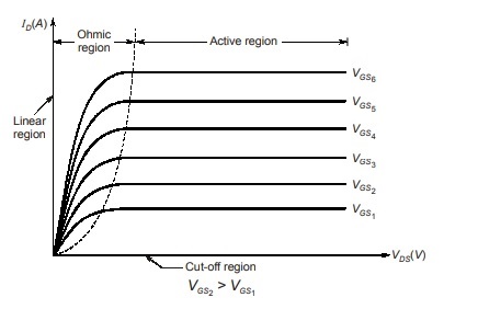
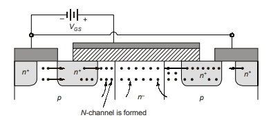
When gate circuit voltage is zero, and VDD is present, n– p junctions are reverse biased and no current flows from drain to source. When gate terminal is made positive with respect to source, an electric field is established and electrons form ‘n’ channel in the ‘p’ region. So a current from drain to source is established. With gate voltage increased, current ID also increases as expected.
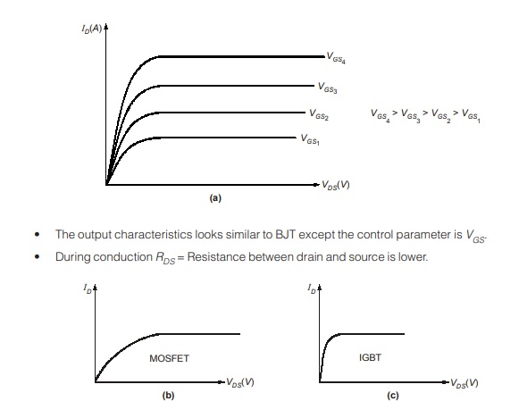
Output Characteristics of Power MOSFET
Power loss of MOSFET during conduction (i.e., ON state)
PL(ON) = I 2DRDS(ON)
NOTE: BJT on state voltage drop is less compared to a MOSFET.
Insulated Gate Bipolar Transistor (IGBT)
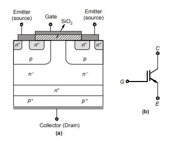
- If we combine the advantage of both BJT and MOSFET an IGBT is constructed.
- It was developed in 1988 by Jayant Baliga.
Operation
When the applied voltage between Gate and source (Emitter) is higher than threshold value a ‘n’ channel is formed near Gate.
So, the electrons will start flowing from n+ region to n–
When the positive voltage is applied between the drain and source, and VGS is greater than threshold value a current Id flows from drain to source.
NOTE: In MOSFET flow of current is only due to flow of electrons, but here in IGBT flow of current is due to electrons and holes.
V-I Characteristics
<< Previous | Next >>
Must Read: What is Power Electronics?
Dear Aspirants,
Your preparation for GATE, ESE, PSUs, and AE/JE is now smarter than ever — thanks to the MADE EASY YouTube channel.
This is not just a channel, but a complete strategy for success, where you get toppers strategies, PYQ–GTQ discussions, current affairs updates, and important job-related information, all delivered by the country’s best teachers and industry experts.
If you also want to stay one step ahead in the race to success, subscribe to MADE EASY on YouTube and stay connected with us on social media.
MADE EASY — where preparation happens with confidence.
MADE EASY is a well-organized institute, complete in all aspects, and provides quality guidance for both written and personality tests. MADE EASY has produced top-ranked students in ESE, GATE, and various public sector exams. The publishing team regularly writes exam-related blogs based on conversations with the faculty, helping students prepare effectively for their exams.