Combinational and Sequential Circuits
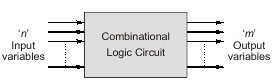
A combinational circuit consists of an interconnection of logic gates, whose outputs at any instant of time are determined from present combination of inputs only. A block diagram of a combinational circuit is shown in figure below. The ‘n’ input binary variables come from external sources; the ‘m’ output variables are produced by the internal combinational logic circuit and go to an external destination. Each input and output variables exist physically as an analog signal whose values are interpreted to be a binary signal that represents logic ‘1’ and logic ‘0’.
A combinational circuit can be described by ‘m’ Boolean functions, one for each output variable. Each output function is expressed in terms of n input variable. A combinational circuit can also be specified by a truth table that lists the output for each combination of input variables.
DESIGN PROCEDURE FOR COMBINATIONAL CIRCUIT
The design of combinational circuits starts from the specification of the design objective and ends in a logic circuit diagram or a set of Boolean functions from which the logic diagram can be obtained. The procedure involves the following steps:
- From the word description of the problem, identify the number of inputs and outputs and then draw a block diagram.
- Draw a truth table such that it completely describes the operation of the circuit for different acombinations of inputs.
- Write down the Boolean expression(s) for the output(s).
- Simplify the Boolean expression using either algebraic or K-map method.
- Implement the simplified expression using logic gates.
<< Previous | Next >>
Must Read: What is Boolean algebra?
Dear Aspirants,
Your preparation for GATE, ESE, PSUs, and AE/JE is now smarter than ever — thanks to the MADE EASY YouTube channel.
This is not just a channel, but a complete strategy for success, where you get toppers strategies, PYQ–GTQ discussions, current affairs updates, and important job-related information, all delivered by the country’s best teachers and industry experts.
If you also want to stay one step ahead in the race to success, subscribe to MADE EASY on YouTube and stay connected with us on social media.
MADE EASY — where preparation happens with confidence.
MADE EASY is a well-organized institute, complete in all aspects, and provides quality guidance for both written and personality tests. MADE EASY has produced top-ranked students in ESE, GATE, and various public sector exams. The publishing team regularly writes exam-related blogs based on conversations with the faculty, helping students prepare effectively for their exams.