Basic Gates
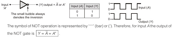
The NOT Gate
- The NOT gate has a single input variable and a single output variable.
- The NOT operation is also referred to as ‘INVERSION’ or ‘COMPLEMENTATION’.
- Thus, its output logic level is always opposite to the logic level of its input.
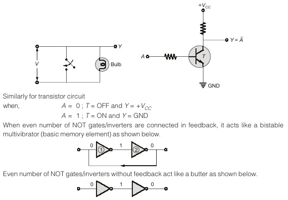
- The switching circuit and transistor circuit for a NOT gate are shown below.
⇒ When switch A is open i.e. logic ‘0’ then, the bulb glows (shows logic ‘1’).
⇒ When switch is closed i.e. logic ‘1’ then, the bulb does not glow (shows logic ‘0’).
Note: Buffers are used to increase the driving capacity of a gate.
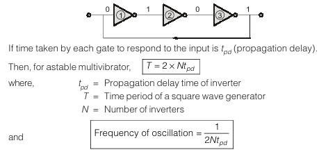
- Odd number of NOT gates/inverters connected in feedback act like an astable multivibrator or, a square wave generator, or a clock pulse generator or, a free running oscillator.
The AND Gate
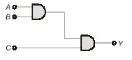
- The AND gate can have two or more inputs but only one output.
- The logic symbol and the truth table of a two input AND gate are,
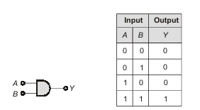
- The logical expression is Y = AB
- It is clear from the truth table that, if all the inputs or any of the input is LOW (logic ‘0’) the output is also at logic ‘0’. However the output is 1 only when all the inputs are 1.
- AND gate follows both commutative and associative law as:
(i) Commutative law: AB = BA
(ii) Associative law: ABC = (AB)C = A(BC)
Enable and disable inputs:
For AND operations
-
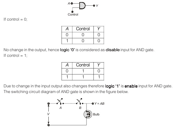 The bulb will glow only when both the switches A and B are closed or at logic ‘1’.
• The AND operation is performed exactly like ordinary multiplication of 1’s and 0’s.
• In multi input AND gate, the unused input can be connected to
(i) Logic ‘1’ or pull up (enable)
(ii) One of the used input
(iii) Left open for TTL logic circuit
Out of these three procedure the best way is to connect the logic ‘1’ or pull up.
Note:
- In ECL logic family, open or floating input will act as logic ‘0’.
- In TTL logic family, open or floating input will act as logic ‘1’.
The OR Gate
- The OR gate can have two or more inputs but only one output. The logic symbol and the truth table for OR gate are,
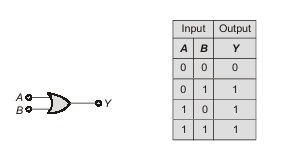
- Thus, the logical expression is Y = A + B
- It is clear from the truth table that, if all the inputs or any of the input is high logic ‘1’ the output Y is HIGH logic ‘1’. Where as if all the inputs are LOW logic ‘0’ then the output Y is low logic ‘0’.
- OR gate follows both commutative and associative laws as:
(i) Commutative law: A + B = B + A
(ii) Associative law: (A + B + C) = (A + B) + C = A + (B + C)
Enable and disable inputs:
For an OR gate
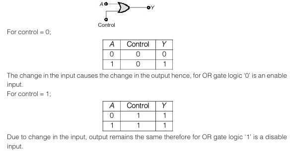
- The switching circuit diagram for OR gate is,
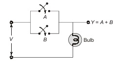
Here, the bulb will glow when any of the switch (either A or B), or both the switches are closed.
- In a multi input OR gate an unused input can be connected to
(i) Logic ‘0’ (Enable) or pull-down.
(ii) Any of the used input.
(iii) Left open or floating in case of ECL logic.
Out of these procedures, the best way is to connected to the logic ‘0’ or pull down.
<< Previous | Next >>
Must Read: What is Boolean algebra?
Dear Aspirants,
Your preparation for GATE, ESE, PSUs, and AE/JE is now smarter than ever — thanks to the MADE EASY YouTube channel.
This is not just a channel, but a complete strategy for success, where you get toppers strategies, PYQ–GTQ discussions, current affairs updates, and important job-related information, all delivered by the country’s best teachers and industry experts.
If you also want to stay one step ahead in the race to success, subscribe to MADE EASY on YouTube and stay connected with us on social media.
MADE EASY — where preparation happens with confidence.
MADE EASY is a well-organized institute, complete in all aspects, and provides quality guidance for both written and personality tests. MADE EASY has produced top-ranked students in ESE, GATE, and various public sector exams. The publishing team regularly writes exam-related blogs based on conversations with the faculty, helping students prepare effectively for their exams.