What is the function of a transistor in an electronic device?
The transistor was invented by Dr. William Shockley and Dr. John Barden at Bell Laboratory in America in 1951. The transistor is a basic building block of all modern electronic systems. It is a three terminal device.
The output voltage, current or power are controlled by the input current in transistor therefore it is called a current controlled device.
BJT stands for Bipolar junction transistor because the transistor operation is carried out by two types of charge carriers majority carriers and minority carriers.
Device Structure
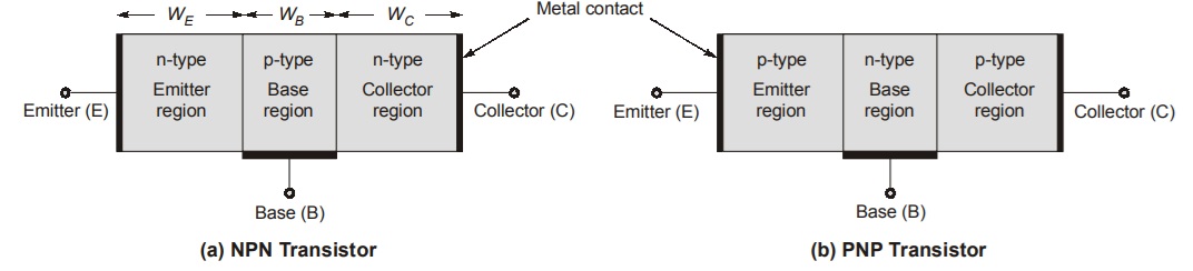
A transistor is a single crystal of Silicon (Si) or Germanium (Ge). A transistor can be of two types: NPN or PNP. It has three separately doped regions and two pn junctions. The junctions are formed by sandwiching either P-type or N-type semiconductor layers between a pair of opposite types as shown in figure below.
The three terminal connections are called emitters, base and collector. The width of the base region is small compared to the minority carrier diffusion length. Generally the sequence of length of the three regions are WB < W E < W C .
Note:
The term transistor was derived from the words TRANSFER and RESISTOR. The term was adopted because it best describes, the operation of a transistor, which is the transfer of an input signal current from a low resistance circuit to a high resistance circuit.
Transistor symbols
There are two types of transistors known as NPN and PNP. The symbols of NPN and PNP are shown below in figure (a) and figure (b) respectively.
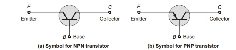
- The symbol for NPN transistor shown in figure (a). The emitter has an arrowhead which indicates the direction of a conventional current flow in a The arrowhead points from P-region towards N-region. Therefore in NPN transistor the conventional current will flow from the base to the emitter.
- The symbols for PNP transistor shown in figure (b). The arrowhead is the emitter points from the P-region towards the N-region. Therefore in a PNP transistor the conventional current will flow from the emitter to the base.
Modes of Operation
The transistor consists of two pn-junctions, the emitter-base junction (EBJ) and the collector-base junction (CBJ). Depending on the bias condition (forward or reverse) of each of these junctions, different modes of operation of BJT are obtained, as shown in Table below.
| S. No. | Mode | EBJ | CBJ | Properties | Applications |
|---|---|---|---|---|---|
| 1. | Cut-off | Reverse bias | Reverse bias | Very high internal resistance | OFF switch |
| 2. | Active | Forward bias | Reverse Bias | Excellent transistor action | Amplifier |
| 3. | Saturation | Forward bias | Forward bias | Very low internal resistance | ON switch |
| 4. | Reverse active | Reverse bias | Forward bias | Very poor transistor action | Attenuator (Practically not used) |
Some Special Diodes
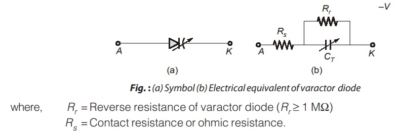
Varactor Diode
- It is a linear graded pn junction diode.
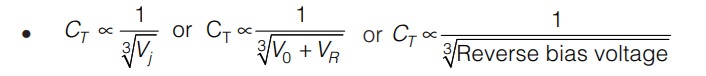
- Its principle of operation is based on transition capacitance CT and operated under reverse bias.
- CT ∝ V–n where n = 1/3 for varactor diode.
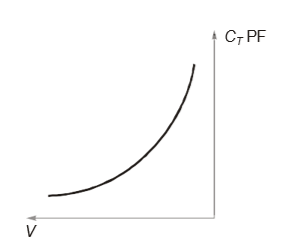
- Capacitance versus reverse bias voltage curve for varactor diode is shown below:
- CT varies as a non-linear function.
- By small variation in reverse bias voltage we get minute change in CT (few pF) therefore major application of varactor diode is in tuning.
- Popularly used material for varactor diode is GaAs.
- It is a low noise microwave device.
 Applications of Varactor Diode
- For direct generation of FM by using diode modulator circuit.
- In designing of voltage control oscillator (VCO) in the PLL circuit.
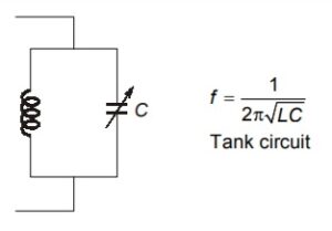
- For tuning of LC resonant circuit.
- For electronic tuning or automatic tuning of receiver.
- For fine tuning of receiver.
- As a special type of amplifier called PARA-amp (parametric amplifier) which is a low noise microwave power amplifier and used with satellite communication.
- For self-balancing of AC bridges.
Tunnel Diode
- It is also known as ESAKI diode.
- Generally operated in the negative resistance region.
- Negative resistance of tunnel diode is due to tunneling effect.
- Negative resistance of tunnel diode is used in designing
-
- Microwave oscillator
- Relaxation oscillator
- Relaxation oscillator is a voltage sweep generator.
- Relaxation oscillator will generate sawtooth voltage waveform and it is applied on horizontal plate of CRT.
- Tunnel diode will exhibit negative resistance property when the device changes its state from ON state to OFF state.
- The operating point or Q-point of tunnel diode is located exactly at the center of the negative resistance region.
- In tunnel diode cut-in voltage is zero.
- In the VI characteristics of tunnel diode, in negative resistance region, tunnel diode will be working as voltage variable negative resistance device.
Disadvantage
- It is a two terminal device therefore no proper isolated output and input section.
- Smaller voltage swing.
Tunneling Effect
“Tunnel diode has a narrow depletion layer and it is almost equal to 1/150th of wavelength of visible light and therefore the charge carrier in the tunnel diode will be penetrating through the narrow depletion layer almost at the speed of light as if there is tunnel in the device and this quantum behaviour of the charge carrier is called tunneling effect.”
V-I Characteristic of Tunnel Diode
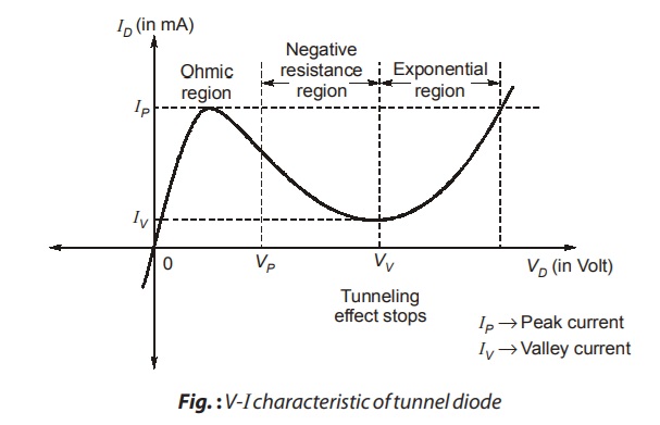
- A reverse bias tunnel diode will be working as a linear device i.e. as a resistor.
- In exponential region, tunnel diode will be working as a normal diode.
- Tunneling current is large at a peak point.
- Tunneling current is small at a valley point.
- Beyond valley voltage tunneling current reduces to zero.
- Diffusion current is small at valley point, beyond valley voltage diffusion current exponentially increases with the voltage.
- Diffusion current is large at the peak point.
- Tunnel diode will exhibit multi-feature property or triple valued property. i.e. any value of forward current between IV and IP can be obtained with three different sets of forward voltages and due to this property tunnel diode is more popular in pulse circuit and also in industrial applications.
- For a good tunnel diode the essential requirements are:
- Larger IP /IV ratio
- Larger voltage swing
Photo Diodes
If a reverse-biased pn-junction is illuminated – that is, exposed to incident light – the photons impacting the junction cause covalent bonds to break, and thus electron-hole pairs are generated in the depletion layer. The electric field in the depletion region then sweeps the liberated electrons to the n-side and the holes to the p-side, giving rise to a reverse current across the junction. This current known as photo-current, is proportional to the intensity of the incident light. Such a diode, called a photodiode, can be used to convert light signals into, electrical signals.
This device consists of a pn-junction embedded in a clear plastic. Radiation is allowed to fall upon one surface across the junction. The remaining sides of the plastic are either painted black or enclosed in a metallic case.
Volt-ampere Characteristics
The reverse saturation current I0 in a pn-diode is proportional to the concentrations of minority carriers in the n and p region. If we illuminate a reverse-biased pn-junction, the number of new hole-electron pairs is proportional to the number of incident photons
Hence the current under large reverse bias is I = I0 + Is, where, Is, the short-circuit current, is proportional to the light intensity. Hence the volt-ampere characteristic is given by
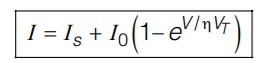
where I, Is and I0 represent the magnitude of the reverse current, and V is positive for a forward voltage and negative for a reverse bias. Typical photodiode volt-ampere characteristics are shown in figure (b). The curves (with the exception of the dark-current curve) do not pass through the origin.
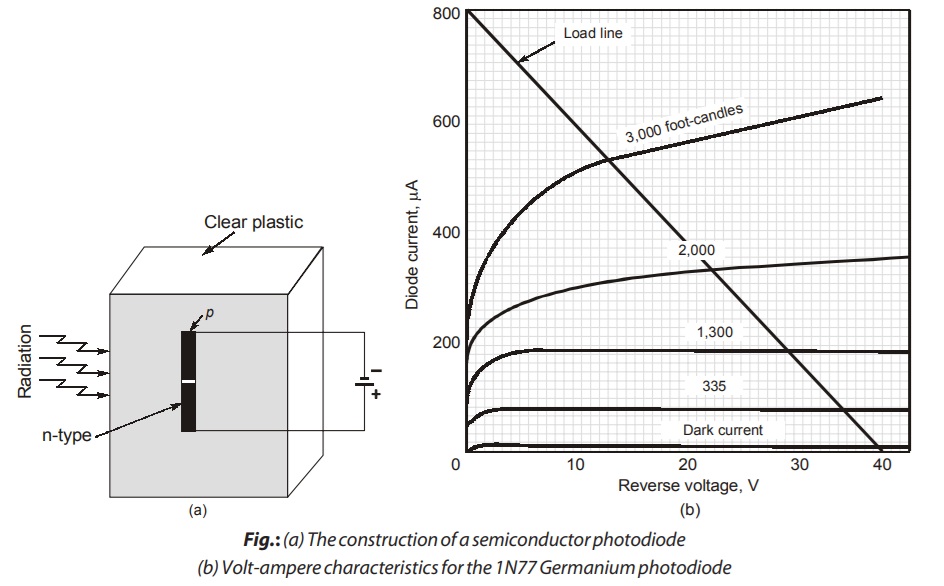
- Dark current is the current when no light is incident on the It corresponds to the reverse saturation current due to the thermally generated minority carriers.
- In photodiode junction is made photo sensitive with the help of photo sensitive materials like CdS, Se and ZnS.
- The operating principle of photodiode is the photoconductive effect (the property where conductivity of a material or device increases with light).
- When compared to normal diode, photodiode is 10 times faster and also has 100 times higher sensitivity.
- Photodiode current is a diffusion current (it is due to the diffusion of injected minority carriers).
Applications
- As a remote control receiver or sensor
- As a light operated switch
- In optocouplers
- To read the audio track recorded on motion picture film
- When photodiode is forward bias and light is focused at the junction:
When photodiode is forward bias, the current is due to majority carriers and it is large (mA). Now if light is focussed at the junction, a number of covalent bonds will be broken and the current in the photodiode further increases but the device can not be operated as a light operated switch.
<< Previous | Next >>
Must Read: What is Electronic Devices and Circuits (EDC)?
Dear Aspirants,
Your preparation for GATE, ESE, PSUs, and AE/JE is now smarter than ever — thanks to the MADE EASY YouTube channel.
This is not just a channel, but a complete strategy for success, where you get toppers strategies, PYQ–GTQ discussions, current affairs updates, and important job-related information, all delivered by the country’s best teachers and industry experts.
If you also want to stay one step ahead in the race to success, subscribe to MADE EASY on YouTube and stay connected with us on social media.
MADE EASY — where preparation happens with confidence.
MADE EASY is a well-organized institute, complete in all aspects, and provides quality guidance for both written and personality tests. MADE EASY has produced top-ranked students in ESE, GATE, and various public sector exams. The publishing team regularly writes exam-related blogs based on conversations with the faculty, helping students prepare effectively for their exams.