Hall Effect
What is Hall Effect?
The Hall effect is a consequence of the forces that are exerted on moving charge by electric field and magnetic field.
Statement
If a specimen (metal or semiconductor) carrying a current-I is placed in a transverse magnetic field B, an electric field E is induced in the direction perpendicular to both I and B. This phenomenon, known as Hall effect, is used to determine whether a semiconductor is n-or p-type and to find the carrier concentration. Also, by simultaneously measuring the conductivity s, the mobility µ can be calculated.
Fig. shown below illustrates the Hall effect. The current-I is in the positive x-direction and B is in the positive z-direction. Electrons and holes flowing in the semiconductor will experience a force. (The force on a particle having a charge q and moving in a magnetic field.) The force is in the negative y-direction independently of whether the carrier are holes or electrons. This charge accumulation induces an electric field in the y-direction. Hence a potential, called the Hall voltage, appears between surfaces 1 and 2.
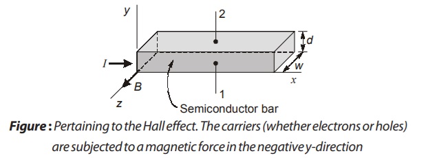
In steady-state, the magnetic field force will be exactly balanced by the induced electric field force or
Usefulness of Hall Effect
- Hall effect is used to determine whether a semiconductor is n-type or p-type.
- It is used to measure majority carrier concentration.
- It is used to measure majority carrier mobility.
Applications
- Magnetofield meter is an instrument operating on the principal of Hall effect and it is used for the measurement of magnetic flux density B.
- Hall effect is also used in Hall effect It gives an output proportional to the product of two signals. If I is made proportional to one of the inputs and if B is linearly related to the second signal, then, VH is proportional to the product of two signals.
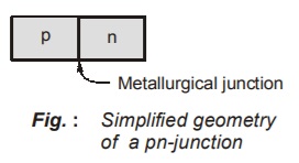
Basic Structure of the p-n Junction
If donor impurities are introduced into one side and acceptors into the other side of a single crystal of a semiconductor as shown in figure. The interface separating the ‘n’ and ‘p’ regions is referred to as the metallurgical junction.
Majority carrier electrons in the n-region will begin diffusing into the p-region and majority carrier holes in the p-region will be diffusing into the n-region. If we assume there are no external excitation to the semiconductor, then this diffusion process cannot continue indefinitely. As electrons diffuse from the n-region, positively charged donor atoms are left behind. Similarly, as holes diffuse from the p-region, they uncover negatively charged acceptor atoms. The unneutralized ions in the neighbourhood of the junction are referred to as uncovered charges. The general shape of the charge density ‘p’ depends upon how the diode is doped. Since the region of the junction is depleted of mobile charges, it is called the depletion region, the space-charge region, or the transition region.
The net positive and negative charges in the n and ‘p’ regions induce an electric fields in the region near the metallurgical junction, in the direction from the positive to the negative charge, or from the n to the p region.
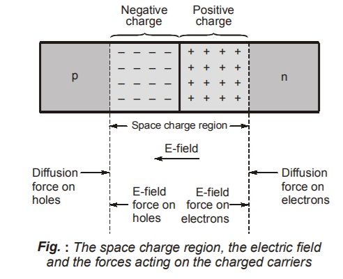
Density gradients still exist in the majority carrier concentrations at each edge of the space charge region and producing a “diffusion force” that acts on the majority carriers as shown in Fig. The electric field in the space charge region produces another force on the electrons and holes which is in the opposite direction to the diffusion force for each type of particle.
In thermal equilibrium, the diffusion force and the electric field force exactly balance each other.
<< Previous | Next >>
Must Read: What is Electronic Devices and Circuits (EDC)?
Dear Aspirants,
Your preparation for GATE, ESE, PSUs, and AE/JE is now smarter than ever — thanks to the MADE EASY YouTube channel.
This is not just a channel, but a complete strategy for success, where you get toppers strategies, PYQ–GTQ discussions, current affairs updates, and important job-related information, all delivered by the country’s best teachers and industry experts.
If you also want to stay one step ahead in the race to success, subscribe to MADE EASY on YouTube and stay connected with us on social media.
MADE EASY — where preparation happens with confidence.
MADE EASY is a well-organized institute, complete in all aspects, and provides quality guidance for both written and personality tests. MADE EASY has produced top-ranked students in ESE, GATE, and various public sector exams. The publishing team regularly writes exam-related blogs based on conversations with the faculty, helping students prepare effectively for their exams.