What is field-effect transistor (FET)
The Field Effect Transistor (FET) is a three terminal device used for a variety of applications. The three terminals of an FET are named as drain (D), Source (S) and Gate (G) out of which gate acts as a controlling terminal.
The field-effect transistor comes in several forms. In a junction FET (Called a JFET) the control (gate) voltage varies the depletion width of a reverse-biased p-n junctions. A similar device results if the junction is replaced by a schottky barrier (metal-semiconductor FET, called MESFET). Alternatively, the metal gate electrode may be separated from the semi conductor by an insulator (metal-insulator-semiconductor FET, called a MISFET). A common special case of this type uses an oxide layer as the insulator (Metal oxide semiconductor FET, MOSFET). The FET is a majority carrier device and is therefore called a unipolar transistor.
Advantages of FET over BJT
FET has several advantages over the conventional bipolar junction transistor.
(i) It is a unipolar device so its operation depends on the flow of majority charge carriers only.
(ii) It is relatively immune to radiation.
(iii) FET has a very high input resistance.
(iv) FET is less noisy.
(v) It does not exhibit any offset voltage at zero drain current hence, it can be used as an excellent signal chopper.
(Vi) FET has a better thermal stability.
Construction of JFETs
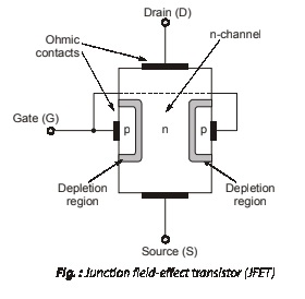
The basic construction of the n-channel JFET is shown in figure below. Note that the major part of the structure is the n-type material, which forms the channel between the embedded layers of p-type material. The top of the n-type channel is connected through an ohmic contact to a terminal referred to as the Drain(D) whereas the lower end of the same material is connected through an ohmic contact to a terminal referred to as the Source(S). The two p-type materials are connected together to the Gate(G) terminal. In essence, therefore, the drain and the source are connected to the ends of the n-type channel and the gate to the two layers of p-type material. In the absence of any applied potentials the JFET has two p-n junctions under no-bias conditions. The result is a depletion region at each region at each junction as shown in figure, that resembles the same region of a diode under no-bias conditions. Recall also that a depletion region is void of free carriers and is therefore unable to support conduction.
Symbols
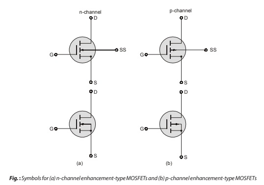
The graphic symbols for the n-channel and p-channel JFETs are provided in figure below. Note that the arrow is pointing in for the n-channel device of Fig. (a) to represent the direction in which IG would flow if the p-n junction were forward-biased. For the p-channel device Fig. (b) the only difference in the symbol is the direction of the arrow.

FET Operation
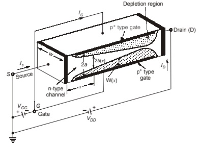
It is necessary to recall that on the two sides of the reverse-biased p-n junction there are space charge regions. The electric lines of field intensity which now originate on the positive ions and terminate on the negative ions are precisely the source of the voltage drop across the junction. As the reverse bias across the junction increases, so also does the thickness of the region of immobile uncovered charges. Hence we see that the effective width of the channel in Fig. will become progressively decreased with increasing reverse bias.
Accordingly, for a fixed drain-to-source voltage, the drain current will be a function of the reverse-biasing voltage across the gate junction. The term field effect is used to describe this device because the mechanism field effect of current control is the effect of the extension, with increasing reverse bias of the field associated with the region of uncovered charges.
MOSFET
The MOSFET compared to BJTs can be made very small (i.e. it requires very less area on an IC). High density VLSI circuits including microprocessors and memories can be fabricated using MOSFET. In the MOSFET the current is controlled by electric field applied perpendicular to both the semiconductors surface and to the direction of current. This phenomenon used to modulate the conductance of a semiconductor, or control the current in a semiconductor, by applying an electric field perpendicular to the surface is called the field effect.
In the following section, we will consider various MOSFETs develop the i-v characteristics. After studying these sections, you should be familiar and comfortable with the MOSFET circuits.
MOSFET Symbols
Comparison between Depletion and Enhancement MOSFET
| Depletion MOSFET | Enhancement MOSFET |
| There is a pre-existing channel
Channel is Diffused channel It can be operated under both depletion and enhancement mode If VGS is kept zero than ID = IDSS Channel is continuous No channel length modulation Relatively larger in size, expensive and also difficult to fabricate due to metallic plate |
No pre-existing channel
Channel has to be created by applying proper VGS Channel is Induced It can be operated only in the enhancement mode When VGS is kept zero than ID = 0 Broken channel Channel length modulation exists Relatively smaller in size, cheaper, economical, easier to fabricate and also provide better performance due to eliminating the metallic plate and using polycrystalline Si material. |
Dear Aspirants,
Your preparation for GATE, ESE, PSUs, and AE/JE is now smarter than ever — thanks to the MADE EASY YouTube channel.
This is not just a channel, but a complete strategy for success, where you get toppers strategies, PYQ–GTQ discussions, current affairs updates, and important job-related information, all delivered by the country’s best teachers and industry experts.
If you also want to stay one step ahead in the race to success, subscribe to MADE EASY on YouTube and stay connected with us on social media.
MADE EASY — where preparation happens with confidence.
MADE EASY is a well-organized institute, complete in all aspects, and provides quality guidance for both written and personality tests. MADE EASY has produced top-ranked students in ESE, GATE, and various public sector exams. The publishing team regularly writes exam-related blogs based on conversations with the faculty, helping students prepare effectively for their exams.