Energy Band Theory of Crystals
The Energy-Band Theory of Crystals
X-ray and other studies reveal that most metals and semiconductors are crystalline in structure. A crystal consists of a space array of atoms or molecules (strictly speaking, ions) built up by regular repetition in three dimensions of some fundamental structural unit. The electronic energy levels discussed for a single free atom (as in a gas, where the atoms are sufficiently far apart not to exert any influence on one another) do not apply to the same atom in a crystal.
When atoms form crystals it is found that the energy levels of the inner-shell electrons are not affected appreciably by the presence of the neighbouring atoms. However, the levels of the outer-shell electrons are changed considerably, since these electrons are shared by more than one atom in the crystal. The new energy levels of the outer electrons can be determined by means of quantum mechanics, and it is found that coupling between the outer-shell electrons of the atoms results in a band of closely spaced energy states instead of the widely separated energy levels of the isolated atom as shown in figure. A qualitative discussion of this energy-band structure follows.
when these atoms are brought into close proximity to form a crystal
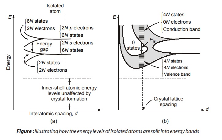
Consider a crystal consisting of N atoms of one of the elements in Table above. Imagine that it is possible to vary the spacing between atoms without altering the type of fundamental crystal structure. If the atoms are so far apart that the integration between them is negligible, the energy levels will coincide with those of the isolated atom. The outer two subshells for each element in Table above contain two s electrons and two p electrons. Hence, if we ignore the inner-shell levels, then, as indicated to the extreme right in Fig. (a), there are 2N electrons completely filling the 2N possible s levels, all at the same energy. Since the p atomic subshell has six possible states, our imaginary crystal of widely spaced atoms has 2N electrons, which fill only one-third of the 6N possible p states, all at the same level.
If we now decrease the interatomic spacing of our imaginary crystal (moving from right to left in Fig. (a), an atom will exert an electric force on its neighbours. Because of this coupling between atoms, the atomic-wave functions overlap, and the crystal becomes an electronic system which must obey the Pauli exclusion principle. Hence the 2N degenerate s states must spread out in energy. The separation between levels is small, but since N is very large (~1023 cm–3), the total spread between the minimum and maximum energy may be several electron volts if the interatomic distance is decreased sufficiently. This large number of discrete but closely spaced energy levels is called an energy band, and is indicated schematically by the lower shaded region in Fig. (a). The 2N states in this band are completely filed with 2N electrons. Similarly, the upper shaded region in Fig. (a) is a band of 6N states which has only 2N of its levels occupied by electrons.
Note that there is an energy gap (a forbidden band) between the two bands discussed above and this gap decreases as the atomic spacing decreases. For small enough distance (not indicated in Fig. (a) but shown in Fig. (b) these bands will overlap. Under such circumstances the 6N upper states merge with the 2N lower states, giving a total of 8N levels, half of which are occupied by the 2N + 2N = 4 N available electrons. At this spacing each atom has given up four electrons to the band; these electrons can no longer be said to orbit in s or p subshells of an isolated atom, but rather they belong to the crystal as a whole. In this sense the elements in Table are tetravalent, since they contribute four electrons each to the crystal. The band these electrons occupy is called the valence band.
If the spacing between atoms is decreased below the distance at which the bands overlap, the interaction between atoms is indeed large. the energy-band structure then depends upon the orientation of the atoms relative to one another in space (the crystal structure) and upon the atomic number, which determines the electrical constitution of each atom. Solutions of Schrodinger’s equation are complicated, and have been obtained approximately for only relatively few crystals. These solutions lead us to expect an energy-band diagram somewhat as pictured4 in Fig. (b). At the crystal-lattice spacing (the dashed vertical line), we find the valence band filled with 4N electrons separated by a forbidden band (no allowed energy states) of extent EG from an empty band consisting of 4N additional states. This upper vacant band is called the conduction band.
Insulators, Semiconductors and Metals
Insulators
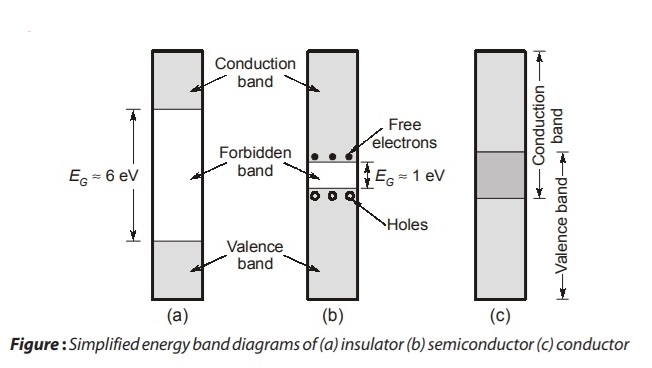
- An insulating material has an energy band diagram as shown in Fig.(a).
- It has a very wide forbidden-energy gap (≃ 6 eV) separating the filled valence band from the vacant
conduction band. Because of this, it is practically impossible for an electron in the valence band to
jump the gap, and reach the conduction band. - At room temperature, an insulator does not conduct. However it may conduct if its temperature is
very high or if a high voltage is applied across it. This is termed as the breakdown of the insulator. - Example: diamond.
Semiconductors
- A semiconductor has an energy-band gap as shown in Fig. (b).
- At 0°K semiconductor materials have the same structure as insulators except the difference in the size of the band gap EG, which is much smaller in semiconductors (EG ≃ 1 eV) than in insulators.
- The relatively small band gaps of semiconductors allow for excitation of electrons from the lower (valence) band to the upper (conduction) band by reasonable amount of thermal or optical energy.
- The difference between semiconductors and insulators is that the conductivity of semiconductors can increase greatly by thermal or optical energy.
- Example: Ge and Si.
Metals
- There is no forbidden energy gap between the valence and conduction bands. The two bands actually overlap as shown in Fig. (c).
- Without supplying any additional energy such as heat or light, a metal already contains a large number of free electrons and that is why it works as a good conductor.
- Example: Al, Cu
Dear Aspirants,
Your preparation for GATE, ESE, PSUs, and AE/JE is now smarter than ever — thanks to the MADE EASY YouTube channel.
This is not just a channel, but a complete strategy for success, where you get toppers strategies, PYQ–GTQ discussions, current affairs updates, and important job-related information, all delivered by the country’s best teachers and industry experts.
If you also want to stay one step ahead in the race to success, subscribe to MADE EASY on YouTube and stay connected with us on social media.
MADE EASY — where preparation happens with confidence.
MADE EASY is a well-organized institute, complete in all aspects, and provides quality guidance for both written and personality tests. MADE EASY has produced top-ranked students in ESE, GATE, and various public sector exams. The publishing team regularly writes exam-related blogs based on conversations with the faculty, helping students prepare effectively for their exams.