Generation of AM Waves
In this section we will discuss the devices and methods used for the generation of standard AM wave based on the nonlinear properties.
The circuit that generates the AM waves is called as amplitude modulator and we will discuss two modulator circuits namely,
- Square law modulator
- Switching modulator
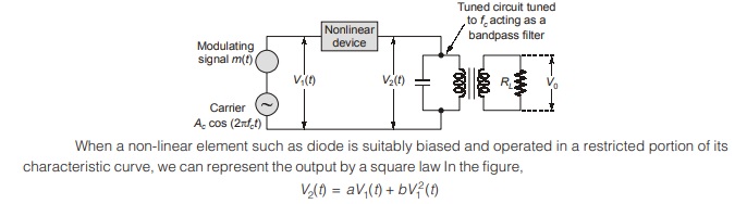
Square-Law Modulator
A square-law modulator requires three features: a means of summing the carrier and modulating waves, a nonlinear element and a band-pass filter for extracting the desired modulation products.
Semiconductor diodes and transistors are the most common nonlinear devices used for implementing square-law modulators. The filtering requirement is usually satisfied by using a single or double tuned filter.
• The square law modulator circuit is as shown in figure below. It consists of the following.
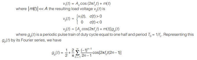
Switching Modulator
A switching modulator is shown in figure below, where it is assumed that the carrier wave c(t) applied to the diode is large in amplitude, so that it swings right across the characteristic curve of the diode. We assume that the diode acts as an ideal switch; that is, it presents zero impedance when it is forward-biased [corresponding to c(t) > 0] and infinite impedance when it is reverse-biased [corresponding to c(t) < 0]
We may thus approximate the transfer characteristic of the diode-load resistor combination by a piecewise linear characteristic, as shown in Figure (b). Accordingly, for an input voltage v1(t) given by
Double-Sideband Suppressed-Carrier Modulation [DSB-SC]
In the standard form of amplitude modulation, the carrier wave c(t) is completely independent of the message signal m(t), which means that the transmission of the carrier wave represents a waste of power. This points to a shortcoming of amplitude modulation; namely that only a fraction of the total transmitted power is affected by m(t). To overcome this shortcoming, we may suppress the carrier component from the modulated wave, resulting in double-sideband suppressed carrier modulation.
The transmitted power is saved here through the suppression of the carrier wave but the channel bandwidth requirement is the same as before (i.e. twice the message bandwidth).
Time-Domain Description
To describe a double-sideband suppressed-carrier (DSBSC) modulated wave as a function of time, we write
s(t) = c(t) m(t)
= Accos (2πfct) m(t)
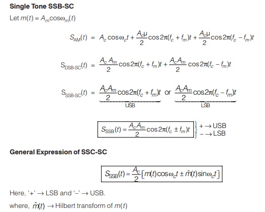
Single Side-Band
SSB-SC Modulation: (Single side Band-suppressed carrier)
So far as the transmission of information is concerned, only one sideband is necessary. So, if the carrier and one side band is suppressed at the transmitter, no information is lost as well as more power is saved. The above modulation technique is referred to SSB-SC modulation.
Derivation of time domain equation of SSB:
Single Tone SSB-SC
Generation of SSB-SC Modulation
Frequency discrimination method or filter method
In this method, first a DSB-SC signal is generated using a simple product modulator and then one of the sidebands is filtered out by an appropriate bandpass filter.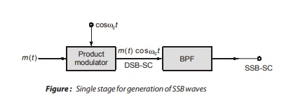
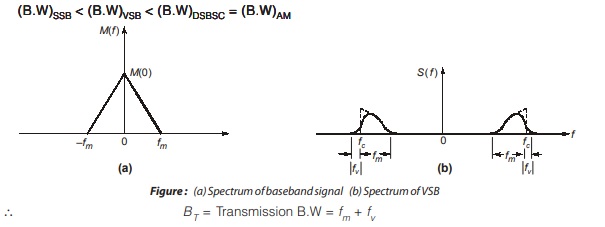
Vestigial Side-band Modulation (VSB)
It is called asymmetric sideband system asymmetric sideband system which is a compromise between SSB and DSBSC modulation.
It is used in T.V. for transmission of picture signal. In this scheme, one side-band is passed almost completely whereas just a trace, or vestige, of the other side band is retained. The transmitted vestige of the unwanted side band compensates for the amount removed from the desired side-band.
Generation of VSB Signal
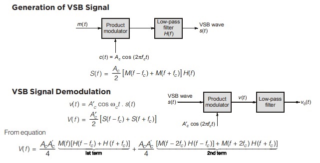
2nd term represents VSB wave with carrier frequency VSB “2 ωc ” and can be filtered out and then produce ” v0(t)
so,
V0(f ) = AcA’c/4 M(f)[H(f – fc) + H(f + fc)]
For the reproduction of the original signal m(t) at the coherent detector output. The transfer function H(ω) of the filter must satisfy the condition,
H(f – fc) + H(f + fc) = 2Hfc
where H(fc) is a constant.
<< Previous | Next >>
Must Read: What is Communication?
Dear Aspirants,
Your preparation for GATE, ESE, PSUs, and AE/JE is now smarter than ever — thanks to the MADE EASY YouTube channel.
This is not just a channel, but a complete strategy for success, where you get toppers strategies, PYQ–GTQ discussions, current affairs updates, and important job-related information, all delivered by the country’s best teachers and industry experts.
If you also want to stay one step ahead in the race to success, subscribe to MADE EASY on YouTube and stay connected with us on social media.
MADE EASY — where preparation happens with confidence.
MADE EASY is a well-organized institute, complete in all aspects, and provides quality guidance for both written and personality tests. MADE EASY has produced top-ranked students in ESE, GATE, and various public sector exams. The publishing team regularly writes exam-related blogs based on conversations with the faculty, helping students prepare effectively for their exams.