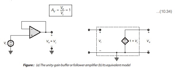
Voltage Follower – Analog Circuits
- An interesting property of non-inverting op-amp occurs when R1 = ∞, an open circuit. The closed loop gain is independent of resistor R2 (except when R2 = ∞), so we can set R2 = 0 to create a short-circuit.
- Since, the output voltage follows the input, this op-amp circuit is called a voltage follower voltage follower.
- The voltage-follower op-amp circuit is shown in the figure. The property of high input impedance is a desirable feature of non-inverting configuration; which enables this circuit to behave as a buffer amplifier to connect a source with high impedance to low-impedance load. The gain of buffer amplifier is
Current-to-Voltage Converter
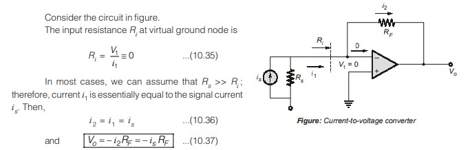
The output voltage is directly proportional to signal current, and the feedback resistance RF is equal to the magnitude of the ratio of output voltage to signal current.
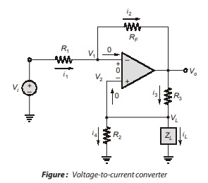
Voltage-to-Current Converter
Consider the circuit given in the figure. The inverting terminal (1) is not at virtual ground. From the virtual
short concept, V1 = V2 and we also note that V1 = V2 = VL = iL ZL. Equating the current i1 and i2, we have
which means that the load current is proportional to input voltage and is independent of the load impedance ZL , as long as the output voltage remains between allowed limits.
Differential Amplifier
An ideal difference amplifier amplifies only the difference between two signals; rejects any common signal to two input terminals. Consider the circuit shown in Figure
(a), with inputs Vi1 and . Vi2 To analyze the circuit, we will use the concept of superposition and virtual short.
(b) shows the circuit with input Vi2 = 0. No current will flow in R3 and R4; therefore, V2a = 0. The resulting circuit will behave as an inverting amplifier so
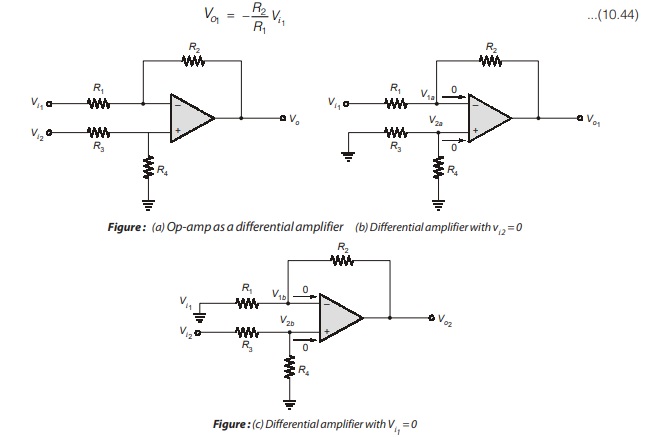
Fig. (c) shows the circuit with Vi1 = 0. Since the current into the op-amp is zero, R3 and R4 form a voltage divider. Therefore,
The differential input resistance of a differential amplifier can be determined by using the circuit shown in the figure. In the figure, we have imposed the condition given in equation (10.50) and have set R1 = R3 and R2 = R4. The input resistance is then defined as
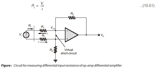
Taking into account the virtual short concept, we can write the following loop equation,
Vi = i R1 + i R1 = i(2 R1)
Therefore, the input resistance is
R1 = 2 R1
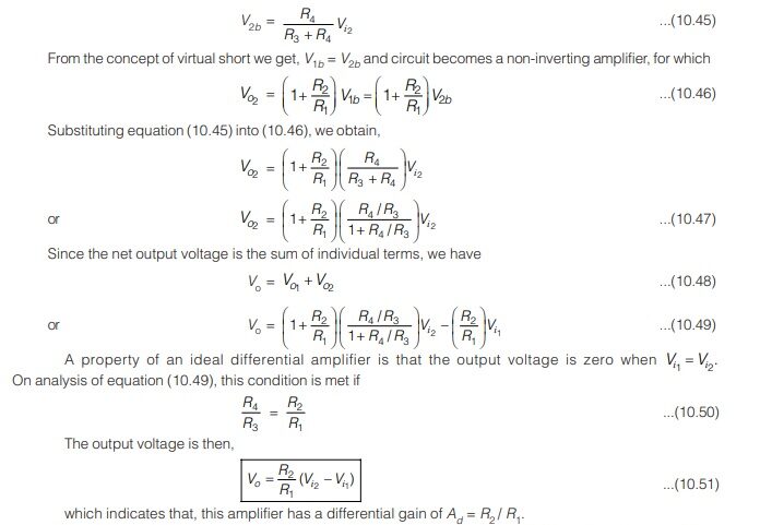
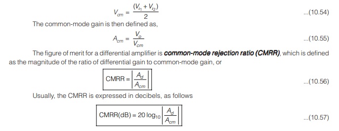
In the ideal difference amplifier, the output v0 is zero when Vi1 = Vi2 However, an inspection of equation (10.49) shows that, this condition is not satisfied if R4/R3 ≠ R2/R1. When Vi1 = Vi2 the input is called common-mode input signal. The common-mode input voltage is defined as .
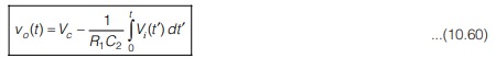
Integrator and Differentiator
Figure shows a generalized inverting amplifier for which the voltage transfer function has similar general form as calculated earlier, that is V0/V1 = -Z2/Z1
where Z1 and Z2 are generalized impedances. Two special circuits can be developed from this generalized inverting amplifier.
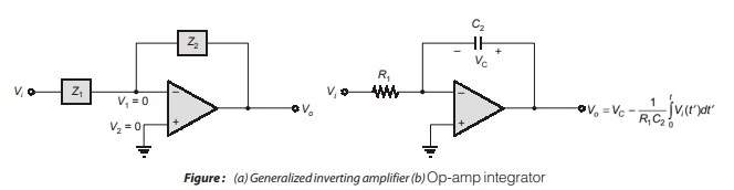
In Figure (b), Z1 corresponds to a resistor and Z2 to a capacitor. The impedance are then Z1 = R1 and Z2 = 1/sC2, where s is the complex frequency. The output voltage is
![]()
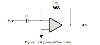
Equation (10.59) represents integration in time domain. If Vc is the voltage across the capacitor at t = 0, the output voltage is
where t′ is the variable of integration. Figure (b) summarizes these results.
The second generalized inverting op-amp uses a capacitor for Z1 and a resistor for Z2, as shown in Figure (c). The impedances are Z1 = 1/sC1 and Z2 = R2, and the voltage transfer function is
Instrumentation Amplifier
In a number of industrial and consumer applications, one is required to measure and control physical quantities. Some typical examples are measurement and control of temperature, humidity, light intensity, water flow etc. These physical quantities are usually measured with the help of transducers. The output of transducer has to be amplified so that it can drive the indicator or display system. This function is performed by an instrumentation amplifier. The important features of an instrumentation amplifier are:
- high gain accuracy
- high CMRR
- high gain stability with low temperature coefficient.
- low DC offset
- low output impedance
- high input impedance
The instrumentation amplifier has high common mode rejection capability that means it can reject a signal that is common to both terminal but amplify a differential signal and this feature is useful for receiving small signals buried in large common-mode offsets or noise.
[There are specially designed op-amps such as µA 725 to meet above stated requirements of a good instrumentation amplifier. Monolithic (single chip) instrumentation amplifiers are also available commercially such as AD521, AD524, AD620, AD624 by Analog Devices, LM-363.XX (XX → 10,100,500) by National Semiconductor and INA101,104, 3636, 3629 by Burr-Brown.]
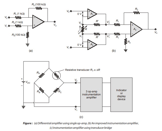
Consider the basic differential amplifier as shown in Figure (a). It can be easily seen that the output voltage V0 is given by,
In Figure (a), source V1 sees an input impedance = R3 + R4 (= 101 kΩ) and the impedance seen by source V2 is only R1 (1 kΩ). This low impedance may load the signal source heavily. Therefore, high resistance buffer is used proceeding each input to avoid this loading effect as shown in Figure (b).
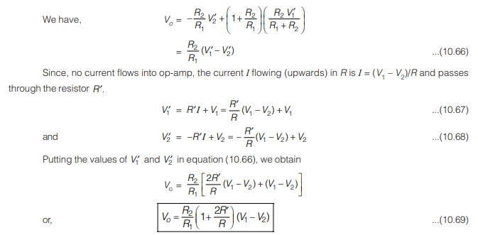
The op-amps A1 and A2 have differential input voltage as zero. For V1 = V2, that is, under common mode condition, the voltage across R will be zero. As no current flows through R and R′ the non-inverting amplifier A1 acts as voltage follower, so its output V’2 = V2. However, if V1 ¹ V2, current flows in R and R’2 , and (V2′ – V1′) > (V2 – V1). Therefore, this circuit has differential gain and CMRR more as compared to the single op-amp circuit of Fig. 10.23 (a). The output voltage Vo can be calculated as follows:
The voltage at the (+) input terminal of op-amp A3 is R2V’1/R1+R2 Using superposition theorem,
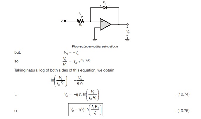
Consider the circuit given in the figure. The diode is to be forward biased, so the input voltage is limited to positive values. The diode current is
iD = Is (eVD/hVT – 1)
If the diode is sufficiently forward biased, the (–1) term is neglected and diode current can be rewritten as
iD = Is eVD/hVT
The input current can be written as,
i1 = Vi/R1
and the output voltage, since voltage at inverting terminal of op-amp is at virtual ground, is given by
V0 = –VD
Noting that i1 = iD, we can write
i1 = Vi/R1 = iD = Is eVD/hVT1
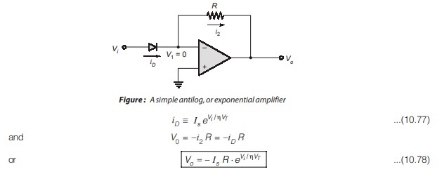
Antilog or Exponential Amplifier
The complement or inverse function of a log amplifier is antilog, or exponential amplifier. A simple example using a diode is shown in the figure. Since V1 is at virtual ground, we can write for V1 > 0
<< Previous | Next >>
Must Read: What are Analog Circuits?
Dear Aspirants,
Your preparation for GATE, ESE, PSUs, and AE/JE is now smarter than ever — thanks to the MADE EASY YouTube channel.
This is not just a channel, but a complete strategy for success, where you get toppers strategies, PYQ–GTQ discussions, current affairs updates, and important job-related information, all delivered by the country’s best teachers and industry experts.
If you also want to stay one step ahead in the race to success, subscribe to MADE EASY on YouTube and stay connected with us on social media.
MADE EASY — where preparation happens with confidence.
MADE EASY is a well-organized institute, complete in all aspects, and provides quality guidance for both written and personality tests. MADE EASY has produced top-ranked students in ESE, GATE, and various public sector exams. The publishing team regularly writes exam-related blogs based on conversations with the faculty, helping students prepare effectively for their exams.
