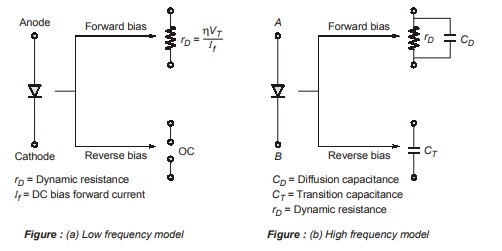
Diode Equivalent Circuits
A diode has 2 types of equivalent circuit
- Small signal model
- Large signal model
Small Signal Model
• If input voltage is small i.e. in mV, then diode is replaced with small signal model.
• Small signal model is again categorised as:
- Low frequency model (Figure (a)).
- High frequency model (Figure (b)).
Remember
- In small signal operation, diode becomes a linear element and diode behaves as resistor.
- The resistance offered by a diode in small signal operation is called as dynamic resistance or small signal resistance OR AC resistance.
- CD is diffusion capacitance present in forward bias when high frequency and small amplitude signal is applied.
CD = τp/rD … for P+N
= τn/rD … for PN+
= τp+τn /rD … for PN
- CT is transition capacitance present in reverse bias when high frequency and small amplitude signal is applied. CT = A∈/W
- where, ∈ = permittivity, W = width of depletion layer and A = Area of junction.
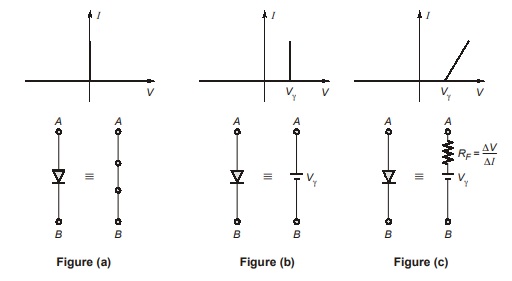
Large Signal Model
• If input voltage is large i.e. in volts, then diode is replaced with large signal model.
• Large signal model is further categorized as:
0th order model (Figure (a))
1st order model (Figure (b))
2nd order model (Figure (c))
Dynamic Resistance of Diode
There are applications in which a diode is biased to operate at a point on the forward i-v characteristics and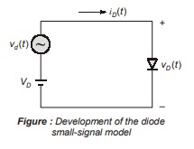 a small ac signal is superimposed on DC quantities. For this situation, we first have to determine the DC operating point (VD and ID). Then, for small signal operation around the DC bias point, the diode is best modelled by a resistance equal to the inverse of the slope of the tangent to the exponential i-v characteristics at the bias point.
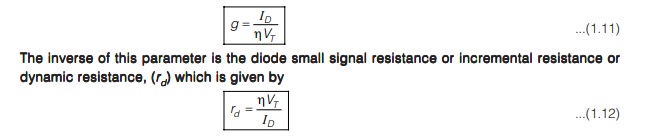
The AC resistance rd takes into account the shape of the curve and represents the slope of the characteristic at the Q-point. If the Q-point changes, the value of rd will also change.
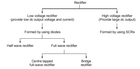
Rectifier
A rectifier that converts an AC voltage to a unidirectional voltage is used as a DC supply for many electronic circuits, such as those in radios, calculators, and stereo amplifiers. A rectifier is also called an AC-DC converter, rectifiers can be classified on the basis of AC supply into two types: single phase rectifiers and three phase rectifiers. Three-phase rectifiers are normally used in higher power applications ; are outside the scope of this book. The following single phase rectifiers are commonly used in electronic circuits:
1. Single phase half-wave rectifiers.
2. Single phase full-wave centre tapped rectifiers.
3. Single phase full-wave bridge rectifiers.
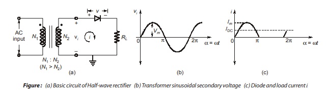
Half-wave Rectifier
The basic circuit for half-wave rectification is shown in Figure (a). We can assume that the diode has essentially infinite resistance in the reverse direction (for a voltage v less than the cut-in voltage Vγ ) and a small and constant resistance Rf in the forward direction (for v > Vγ ). Since in a rectifier circuit the input vi = Vm sinωt has a peak value Vm which is very large compared with the offset voltage Vγ , we assume in the following discussion that Vγ = 0. Subject to this idealization of the diode characteristic, the current i in the diode or load (RL) is given by

Centre-Tapped Full-wave Rectifier
The circuit of a center-tapped full-wave rectifier is shown in Figure (a). This circuit is seen to comprise two half-wave circuits which are so connected that conduction takes places through one diode during one half of the power cycle and through other diode during the second half of the power cycle.
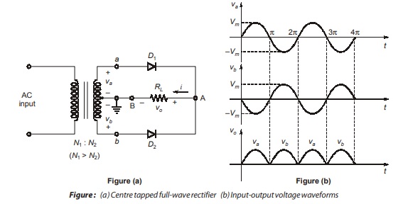
In this rectifier center-tapped step down transformer has been used, in which secondary winding is divided into two halves, each half having equal number of turns. In N1 : N2 center-tapped transformer, primary winding has N1 turns and each half of secondary winding has N2 turns.
When center terminal of secondary winding is grounded, voltage at nodes a and b will have equal magnitude but opposite sign;
Vb = –va
if, va = Vm sinα
then, vb = –Vm sinα
Advantage of Fullwave Rectifier
Following are the advantages of fullwave rectifier over half-wave rectifier:
• Smaller ripple factor.
• Greater efficiency.
• Greater dc output voltage and current.
• Greater transformer utilization factor.
• Filtering of ac component is easier because fundamental frequency (f0) has already been eliminated by the rectifier.
Drawbacks of Fullwave Rectifier
Following are the disadvantages of the fullwave rectifier:
• Higher peak inverse voltage.
• It is necessary to use a center-tapped transformer which is expensive and bigger in size.
Bridge Rectifier
The fullwave rectifier circuit requires a center-tapped transformer where only one half of the total ac voltage of the transformer secondary winding is utilized to convert into dc output. We now consider a different configuration of fullwave rectifier circuit, called bridge rectifier, where entire AC voltage of the transformer secondary is used to convert into DC voltage.
Figure (a) shows a bridge rectifier circuit. There are four diodes D1, D2, D3 and D4 which form the four arms of the bridge. AC from transformer secondary is fed to two corners and the load resistance RL is connected to other two corners. The waveforms for the input and output voltages are shown in figure (b).
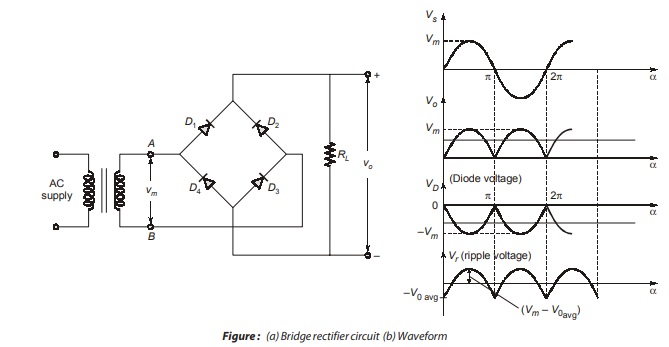
During positive half-cycle of input point A is positive, diodes D1 and D3 are forward biased and diodes D2, D4 are reverse biased then, the current flows through diode D1, the load RL and through diode D3 back to the negative polarity of the transformer secondary. During negative half cycle of input, point ‘B’ is more positive than point ‘A’, thus diodes D2, D4 are forward biased and diode D1 and D3 are reverse biased, then the direction of current flow will be through diode D2, load RL and diode D4. In both cases the current flowing through resistor RL is in same direction, thus it is unidirectional current and we obtain fullwave rectification.
Advantages of Bridge Rectifier
- The current in both primary and secondary of transformer flows for entire cycle and hence for the given power output, transformer of a small size and less cost may be used.
- A transformer without a center tap is used.
- Lower peak inverse voltage is required. The bridge circuit is thus suitable for high voltage applications.
For example, if the peak output voltage is 50 V, the peak inverse voltage across each diode is also 50 V. However, if a fullwave circuit were used, the peak inverse voltage would be 100 V. - It provides greater TUF.
Disadvantage of Bridge Rectifier
The only disadvantage of bridge rectifier is the use of four diodes as compared to two diodes for center tapped FWR. This reduce the output voltage.
Filter
Filter is a frequency selective network which passes a range of frequency and rejects unwanted frequency.
The rectifier output voltage Vo has a DC component and other cosine components at various frequencies. The magnitude of cosine components are called the harmonics. The output should ideally be pure DC, so these frequencies are undesirable. Filters are normally used to smooth out the DC voltage. Since, input is DC, they are known as DC filters. Four types of filters are normally used.
1. Inductor filter
2. Capacitor filter
3. LC filter
4. CLC filter
Inductor and LC filters are generally used for high power applications, such as DC power supplies. For integrated circuits capacitor filters are used.
Inductor Filter
Consider below figure in which a large inductor is connected in series with the load resistance to eliminate the ac component.
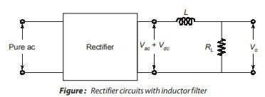
For this circuit inductor should be selected such that its reactance is much higher than RL at the smallest frequency of ac component
i.e. ωoL >> RL for HWR
and, 2 ωoL >> RL for FWR and bridge rectifier
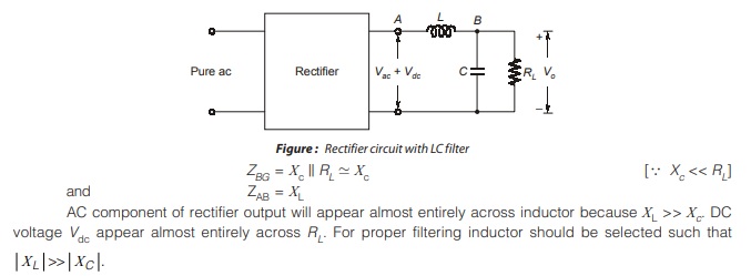
As inductor and RL are in series so they form voltage divider network. Since , |XL| >> RL so Vac appears almost across inductor and negligible ac voltage appears across RL . DC voltage appears across RL because inductor is short circuit for dc.
Capacitor Filter
A capacitor is an energy storage element. It tries to maintain a constant voltage, thereby preventing any change in voltage across the load.
Consider figure below in which a large capacitor is connected in parallel with the load resistance to eliminate AC component.
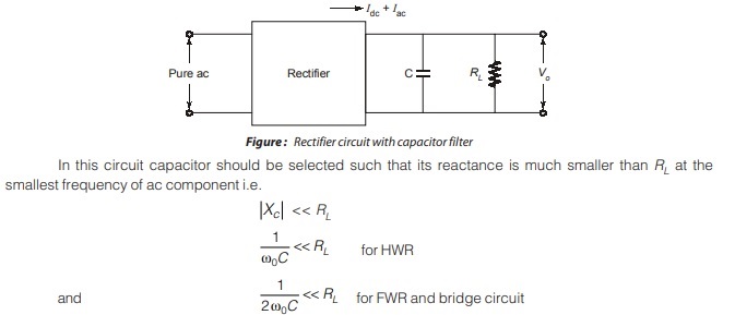
As capacitor and RL are in parallel so they form a current divider circuit. Since |Xc|<< RL so AC component Iac flows almost through the capacitor and very small ac current goes through RL . Since capacitor behaves as open circuit for dc component so IDC flows through RL
LC Filter (L-Section Filter)
An LC filter which opposes any change in either the voltage or current, reduces the harmonics more effectively, than an L-filter or a C-filter.
Consider the figure shown below in which a large inductor and a large capacitor are connected in the form of L-section.
CLC Filter (Π-Section Filter)
- It consists of two capacitors and one inductor which are connected in the form of Π-section.
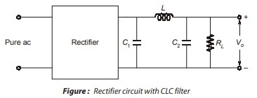
- Above circuit is equivalent to interconnection of rectifier with capacitor filter and followed by LC filter. Voltage across C1 is a triangular waveform whose dc component is given by Vdc = Vm – Vr/2, and ac component has peak to peak value equal to Vr.
- The ac component of Vc1 appears almost across inductor because reactance of inductor is much higher than (XC ||RL). DC component of Vc1 appears almost across RL.
- CLC filter has least ripple factor among all types of filters ; which is given by
- Reactance should be found at ω0 for HWR and at 2ω0 for FWR.
- Also dc output voltage is given by
Vdc = Vm – Vr/2 – IdcRinductor
where, Rinductor is inductor coil resistance.
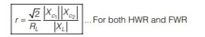
Bleeder Resistor (RB)
It is used in high voltage dc supplies to provide discharge path for capacitor when RL is not present. In absence of bleeder resistor a large dc voltage will be present across capacitor even when the ac supply is turned-off. This high dc voltage across capacitor can cause electric shock if someone touches the plate of capacitor. Bleeder resistor is also used in LC filter so that the inductor current can bleed (or flow) through bleeder resistance RB, if RL is not present. With the help of following figure where bleeder resistance RB is used in CLC filter we will try to summarize the purpose of bleeder resistor in filter circuits.
RB > > RL
- The value of bleeder resistance should be such that it draws only 10% of total load current.
- It provides better voltage regulation.
- It provides safety to operator by providing discharge path to the capacitor.
- Single power supply can be used to provide more voltage.
- Bleeder resistance can be used as voltage divider for tapping out any desired output.
Voltage Regulators
Regulator is an electronic circuit which maintains DC output voltage of a power supply stable or constant irrespective of fluctuations in ac supply and variations in load current.
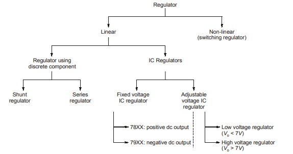
Zener Diode Shunt Regulator
Below figure represents a Zener diode shunt regulator.
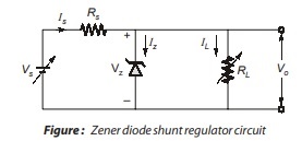
Here
Vs = Unregulated supply voltage (fluctuating dc output voltage of filter)
Rs = Series current limiting resistor which prevents flow of heavy current through diode
As there is parallel connection of Zener diode and load RL , so the circuit is known as shunt regulator.
Here, Vo = Vz
and, Is = Vs-Vz/Rs
also, Is = IZ + IL
Clipper
Clipping circuits are used to select for transmission that part of an arbitrary waveform, which lies above or below some particular reference voltage level clipping circuits are also referred to as voltage limiters, amplitude selectors or slicers.
Diode clipper are the networks, which employ diodes to “clip” away a portion of an input signal without distorting the remaining part of the applied waveform.
Applications
- It is used to limit the amplitude of a signal therefore clipper is also called “amplitude limiter”.
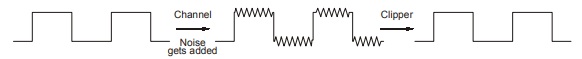
- A clipper can be used to eliminate noise from pulse waveforms in digital communication.
- Clippers are classified into two-parts
1. Shunt clipper: A clipper in which the diode is connected across the output terminals or diode is connected parallel to the load is known as shunt or parallel-clipper.
2. Series clipper: A clipper in which diode forms a series circuit with the output terminals is known as a series clipper.
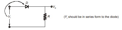
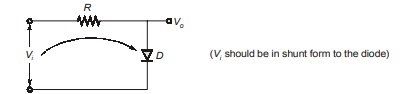
Shunt Clipper
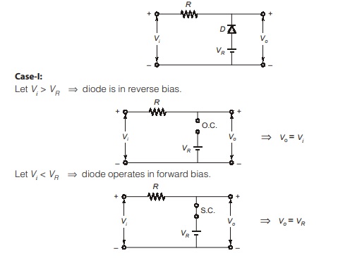
Below figure shows a shunt clipper. Here VR is the reference voltage and R is the current limiting resistance. Resistance R should not be too large or too small. For proper clipping operation R should be calculated as follows:
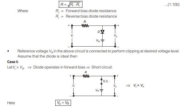
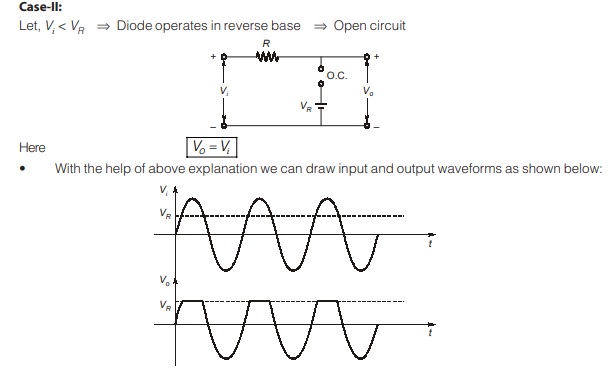
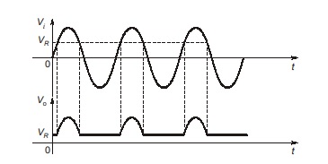
- Hence we see that the circuit removes a portion of the input signal which lies above reference voltage. This operation is called clipping above reference.
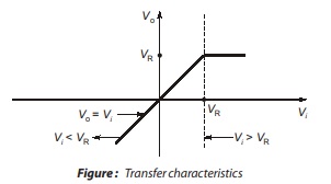
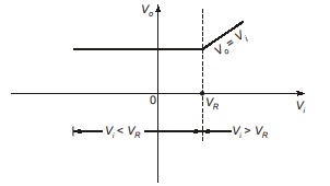
Transfer Characteristics:
It is a graph plotted between output voltage and input voltage.
Note:
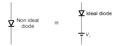
If a diode is non-ideal or it has cut-in voltage equal to Vγ then this diode should be replaced with a series connection of ideal diode and a battery of Vγ
Consider another type of the clipper circuit, in which direction of diode is reversed, then clipping becomes opposite of the previous clipper.
- Above circuit removes a portion of input signal which lies below the reference voltage. This operation is called clipping below the reference
Transfer Characteristics:
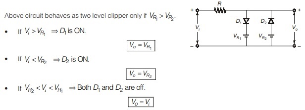
Two level clipper
This circuit performs clipping at two independent voltage levels. It consists of two diodes and two reference voltages connected as shown below:
Clamper
A clamper is a network consisting of a diode, resistor, and capacitor that shifts a waveform to a different dc level without changing the appearance of the applied signal. A clamper is also used to reinsert or restore dc component into a waveform which has been lost after passing through a processing network such as an amplifier. Hence a clamper is also called dc reinserter or dc restorer.
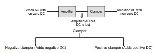
Note: Amplifiers have blocking capacitor which blocks the DC components.
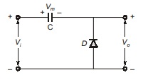
Negative Clamper
Negative clamping occurs when positive peak raised or clamped to ground or on zero level, in the other words, it pushes the signal downwards so that positive zero level.
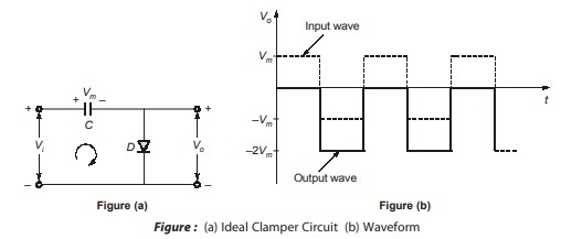
When input is positive, diode operates in forward bias and capacitor charges through diode. If diode is ideal it behaves as short circuit and therefore capacitor charges upto the peak input Vm
When input becomes negative capacitor should discharge but discharge path is not available so capacitor voltage will continue to remain Vm. Therefore once capacitor is fully charged its voltage remains Vm irrespective of the input being positive or negative.
KVL:
–Vi+ Vm + V0 = 0
Vo = Vi – Vm
Vo = Vi + (–Vm)
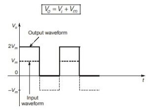
Hence circuit adds dc voltage of –Vm. So output will be a square waveform for given input whose value varies from 0 to –2 Vm. Positive peak of output waveform touches 0 volt level or positive peak gets clamped to 0 volt. Since a negative clamper is clamping positive peak to 0 volt so it is also called positive peak clamper.
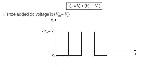
- If diode has cut-in voltage Vγ then it should be replaced with series connection of ideal diode and battery Vγ
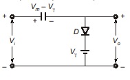
When input is positive capacitor charges through diode upto a maximum voltage of Vm – Vγ
V0 = Vi – (Vm – Vγ)
V0 = Vi + (–Vm + Vγ)
Hence circuit adds dc voltage equal to –(Vm – Vγ).
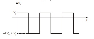
Hence when diode is non-ideal negative clamper will clamp positive peak to Vγ
Drawbacks of Ideal Clamper
- As capacitor does not have discharge path so its voltage can not decrease even when the peak ac input is
 reduced which makes this clamping operation imperfect.
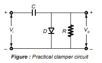
 - To overcome the above drawback a sufficiently large resistance should be connected in shunt with the diode such a circuit is called practical clamper.
- When peak input is reduced, capacitor slowly discharges through resistance R and after a finite time interval its voltage becomes equal to new peak value.
- R should be large enough so that capacitor does not have undesired discharging when peak input is stable.
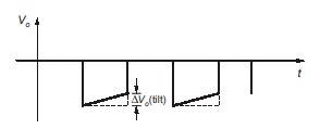
Drawback of Practical Clamper
During negative cycle diode will be in off condition then capacitor slowly discharges through resistance R as a result capacitor voltage decreases and tilt appear in output waveform.
Note:
- In a practical clamper, R is selected such that the discharging time constant is much greater than time period of input.
i.e. RC >> T0
- If discharging is rapid, then circuit will not act as CLAMPER.
Positive Clamper
Positive clamping occurs when negative peaks raised or clamped to ground or on zero level. In other words, it pushes the signal upwards so that negative peaks fall on the zero level.
- When input is negative diode gets forward biased and capacitor charges through diode upto peak input Vm
- When input becomes positive capacitor will not be able to discharge as discharge path is not present ; therefore voltage across the capacitor remains Vm irrespective of input being +Vm or –Vm.
KVL:
- Negative peak of output gets clamped to 0 volt therefore positive clamper is also called negative peak clamper
- If diode has cut-in voltage Vγ then capacitor charges to a voltage (Vm – Vγ). Applying KVL again
Here negative peak gets clamped to –Vγ
Voltage Multiplier
A circuit whose input is an ac waveform of peak value Vm and output is dc voltage which is an integral multiple of peak ac input i.e. Vo = 2 Vm, 3 Vm, 4 Vm etc. is called a voltage multiplier.
Vo = DC voltage of 2 Vm ⇒ Voltage doubler
Vo = DC voltage of 3 Vm ⇒ Voltage tripler
Vo = DC voltage of 4 Vm ⇒ Voltage quadrupler
It is an AC-DC inverter, made up of diodes and capacitors that produce high DC output from a low voltage AC input.
Voltage Doubler
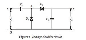
Vi is any ac waveform. Let us assume that it is a square waveform of amplitude ±Vm.
- Case-I:
When input is negative D1 gets forward bias then capacitor C1</sub charges through D1 upto voltage Vm - Case-II:
If Vi is positive or + Vm
then VAG = Vm + Vm = 2 Vm
D2 operates in forward bias and C2 charges through D2 upto voltage 2 Vm. - If capacitors are fully charged or circuit is in steady state then voltage Vm will be present across C1
and 2 Vm across C2. Thus
Vo = DC voltage of 2Vm
Voltage Tripler/Quadrupler
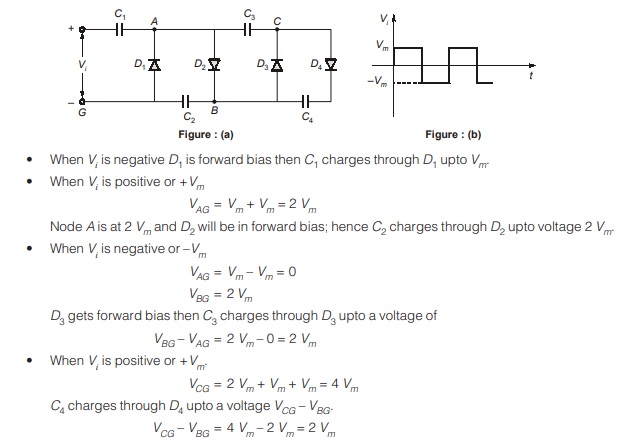
In steady state voltage Vm is present across C1 and voltage 2 Vm is present across other three capacitors.
DC voltage of 4 Vm can be obtained if Vo is measured across C4 and C2 combination.
DC output of 3 Vm can be obtained if Vo is measured across C3 and C1 combination.
<< Previous | Next >>
Must Read: What are Analog Circuits?
Dear Aspirants,
Your preparation for GATE, ESE, PSUs, and AE/JE is now smarter than ever — thanks to the MADE EASY YouTube channel.
This is not just a channel, but a complete strategy for success, where you get toppers strategies, PYQ–GTQ discussions, current affairs updates, and important job-related information, all delivered by the country’s best teachers and industry experts.
If you also want to stay one step ahead in the race to success, subscribe to MADE EASY on YouTube and stay connected with us on social media.
MADE EASY — where preparation happens with confidence.
MADE EASY is a well-organized institute, complete in all aspects, and provides quality guidance for both written and personality tests. MADE EASY has produced top-ranked students in ESE, GATE, and various public sector exams. The publishing team regularly writes exam-related blogs based on conversations with the faculty, helping students prepare effectively for their exams.