Bipolar Junction Transistors-Characteristics and Biasing
Bipolar Junction Transistors
Three-terminal devices are far more useful than two-terminal ones, such as diodes studied earlier in chatper-1, because they can be used in a multitude of applications, ranging from signal amplification to designing of digital logic and memory circuits. The basic principle involved is the use of the voltage between two terminals to control the current flowing in the third terminal. In this way, a three terminal device can be used to realize controlled source, which is the basic for amplifier design. Also, in extreme, the control signal can be used to cause current in third terminal to change from zero to a large value, thus allowing the device to act as a switch.
The transistor consists of two pn-junctions, the emitter emitter-base junction (EBJ) and the collector the collector-base junction (CBJ). Depending on the bias condition (forward or reverse) of each of these junctions, different modes of operation of BJT are obtained, as shown in Table.
| S. No. | Mode | EBJ | CBJ | Properties | Applications |
|---|---|---|---|---|---|
| 1. | Cut-off | Reverse bias | Reverse bias | Very high internal resistance | OFF switch |
| 2. | Active | Forward bias | Reverse Bias | Excellent transistor action | Amplifier |
| 3. | Saturation | Forward bias | Forward bias | Very low internal resistance | ON switch |
| 4. | Reverse active | Reverse bias | Forward bias | Very poor transistor action | Attenuator (Practically not used) |
Table : BJT Modes of Operation
- Mode refers to the way how two junctions of BJT are biased.
- As we will see shortly, charge carriers of both polarities—that is, electrons and holes—participate in the current conduction process in a bipolar transistor, which is the reason for naming it bipolar bipolar.
Device Structure
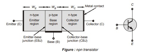
The bipolar transistor has three separately doped regions and two p-n junctions. Figure shows the basic structure of an npn bipolar transistor and pnp bipolar transistor, along with the circuit symbols. The three terminal connections are called the emitter emitter, base and collector collector. The width of the base region is small compared to the minority carrier diffusion length. Generally the sequence of length of the three regions are WB < WE < WC.
Note:
An important point to note from the devices shown in figure is that bipolar transistor is not a symmetrical device. Although the transistor may contain two n-regions or two p-regions, the impurity doping concentrations in the emitter and collector are different and the geometry of these regions can be vastly different.
There are few specific features that differentiate one region from the other region. That are
Emitter Region
- A region which supplies or emits majority carriers, for example in pnp transistor emitter will supply holes and in npn transistor it supplies electrons.
- Emitter is heavily doped, so that it can emit large number of carriers.
- Impurities are added in the ratio 1 : 103.
Collector Region
- A region which receives or collects majority carriers coming from emitter.
- It is moderately doped and largest in size.
- Large collector will help in rapid transfer of heat to the surroundings.
- In a transistor collector junction develops large amount of heat because it operates at higher current and higher voltage.
- If collector is lightly doped it’s conductivity will decrease, which is undesired.
- If collector is heavily doped breakdown voltage of collector junction will decrease which is also undesired. Therefore collector is moderately doped so that it has better conductivity and collector junction has higher breakdown voltage.
Base Region
- A region through which majority carriers travel from emitter to collector.
- Base is lightly doped and small in size, i.e. it has narrow width (10–6 m).
- The number of electron-hole recombination inside base will be reduced by keeping it narrow in width and by doping it lightly.
- Impurities are added in ratio 1 : 108.
Early Effect 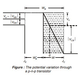
When BJT is biased in active region the emitter junction (JE) is forward-biased but the collector junction is reverse-biased, then in figure the barrier width at JE is negligible as compared to space charge width W at JC.
The transition region at junction is a region of uncovered charges on both sides of junction at positions occupied by impurity atoms. As the voltage applied across the junction increases, transition region penetrates deeper into collector and base. As neutrality of charges must be maintained, so the number of uncovered charges on each side remains equal. Since the doping in base is substantially smaller than that of collector, the penetration of the transition region into the base is much larger than that in collector. Hence the collector depletion region is neglected in figure, and all immobile charges are indicated in base region.
If metallurgical base width is WB, then the effective electrical base width is . W’B = WB – W. This modulation of effective base width by reverse bias VCB is known as the Early effect Early effect or Base width modulation.
Consequences of Early Effect
The decrease in W’B with increase in reverse collector voltage has three consequences.
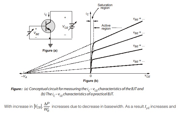
1. When |VCB| is increased the effective base width of transistor decreases so there are less chances of recombination of charge carriers within the base region. As a result α increases with increasing |VCB|.
2. With decrease in base width the concentration gradient of minority carriers is increased within the base. As we have,
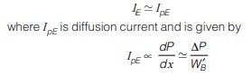 where W’B is effective basewidth.
consequently IE also increases. Hence we see that IE increases due to increase in gradient of concentration of holes.
Also in BJT, voltage applied across one junction has effect on current passing through other junction therefore junctions JE and JC are called interactive junctions.
3. At large value of |VCB| depletion region can fully occupy the base region or in other words for extremely large voltages, W’B may be reduced to zero. This phenomenon is known as punch through or reach through.
When punch-through occurs effective base width becomes zero and collector region gets electrically shorted to emitter. Due to this shorting, the negative voltage applied at collector reaches emitter also. This results in heavy current flow which can damage the transistor.
Instability in Collector Current
In the preceding section we have seen that for faithful reproduction of the input signal we need a stable Q-point. In other words we can say that dc collector current should be fixed in a particular circuit. But as we know that collector current can be given by the following equation:
IC = βIV + (1 + β)ICO
IC can be unstable due to following reasons.
1. Variations in ICO :
ICO is reverse saturation current of collector junction. It increases with increase in temperature due to increase in the concentration of minority carriers
If temperature increases by 1°C then ICO increases by 7%
For each 10°C rise in temperature ICO doubles.
Hence we see that variation in temperature causes change in ICO and as a result IC also varies.
2. Variations in VBE:
VBE is forward voltage of emitter junction. When temperature increases by 1°C, VBE decreases by 2.5 mV.
![]()
Hence changes in temperature create change in VBE due to which base current (IB) changes. Hence, from above equation we conclude that collector current IC also varies.
3. Variations in β:
β varies either due to transistor replacement or due to variations in temperature.
(a) When a transistor is replaced with another transistor, β value will vary because it is practically difficult to find two transistors having exactly equal β.
(b) For a given transistor β also increases with increase in temperature.
- Hence from above discussion we conclude that Ic is unstable due to variations in Ico, β, and VBE i.e.
Ic = f(Ico, VBE, β)
“The above equation is read as Ic is a function of Ico, β and VBE.”
By using partial differentiation, we have
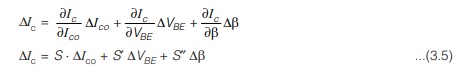
where S, S′ and S″ are the stability factors.
From above equation we conclude that for greater stability in Ic, ∆Ic should be smaller which is possible when stability factors are smaller.
Instability in Ic has two undesired effects:
(a) Operating point will drift or vary along the load line which may result in distorted output and in worst case operating point may move into saturation or cut-off region.
(b) Thermal runaway may occur which damages a BJT.
Hence collector current (Ic) should be made stable with either stabilization or compensation methods.
Calculation of Stability Factor (S)
Stability factor (S) is rate of change of Ic with respect to reverse saturation current Ico,
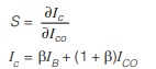
Differentiating above equation with respect to Ic assuming β and VBE are constant
BJT Biasing
Biasing refers to providing appropriate DC voltages and DC currents to an electronic device to operate it in a desired way. Biasing of BJT is done for following purposes:
(i)To operate the BJT in active region so that it can be used as an amplifier.
(ii) To maintain Ic stable so that operating point does not drift and thermal runaway cannot take place.
Commonly used biasing circuits are:
(i) Fixed bias circuit.
(ii) Collector to base bias circuit.
(iii) Self bias circuit.
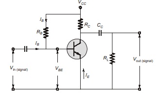
Fixed Bias Circuit
In figure below, the base current is derived from supply voltage Vcc by resistor RB. This type of biasing is called fixed bias as Vcc and RB are fixed quantities.

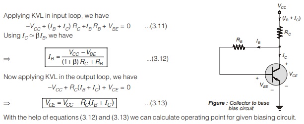
Collector to Base Bias Circuit
An improvement in bias stability is obtained if tapping for bias is taken from the collector terminal instead of from the collector supply point as shown in figure.
Stability Factor
To calculate stability factor, differentiating equation (3.11) with respect to IC ; we have
∂IB/∂IC= -RC/RB + RC
Putting above value in equation (3.7), we have
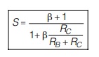
Advantage
Here stability factor is smaller than (β + 1), hence an improvement in stability is obtained over fixed bias circuit.
Disadvantage
- Stability factor depends upon RC. If RC becomes smaller or zero then stability factor becomes very large and IC does not remain stable.
- Resistance RB connected from collector to base causes negative feedback due to which voltage gain of the amplifier circuit decreases.
Self-Bias, Emitter Bias, or Voltage-Divider Bias
If the collector resistance RC is very small, for example, in a transformer-coupled circuit, then from equation (3.14)
we see that there is no improvement in stabilization in collector-to-base bias circuit over the fixed-bias circuit. A circuit which can be used even if there is zero DC resistance in series with the collector terminal is self-biasing configuration of Figure (a). The current in resistance Re in emitter lead causes a voltage drop which is in direction of reverse-biasing the emitter junction. Since this junction must be forward-biased, the base voltage is obtained from supply through R1, R2 network. Note that if Rb= R1 || R2 → 0, then base to ground voltage VBN is independent of ICO. Under these circumstances we may verify that S = ∂IC/∂ICO → 1
For best stability R1 and R2 must be kept as small as possible.
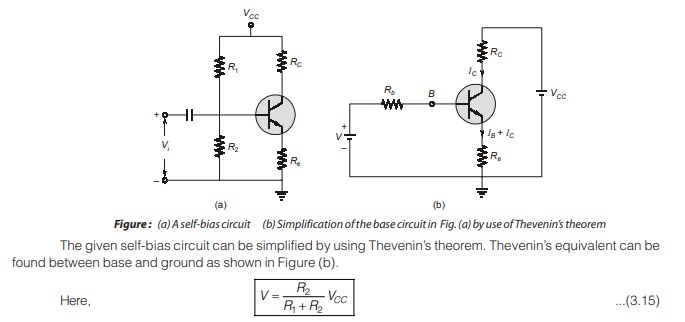
By using equations (3.18) and (3.19) we can easily calculate operating point for self-bias circuit.
Stability Factor
To calculate stability factor, differentiate equation (3.17) with respect to IC

- Note that S varies between 1 for small Rb/Re and 1 + β for Rb/Re → ∞.
- Smaller the value of Rb, better is stabilization. Note that even if Rb approaches zero, the value of S can not be reduced below unity. Hence Ic always increases more than Ico.
- As Rb is reduced while Q-point is held fixed, the current drawn in R1, R2 network from supply VCC increases.
- Also, if Re is increased while Rb is held constant, then to operate at the same quiescent current, the magnitude of VCC must be increased.
- In either case a loss of power (decreased efficiency) is disadvantage which accompanies the improvement in stability.
- In order to avoid the loses of AC (signal) gain because of feedback caused by Re, this resistance is often bypassed by a large capacitance (> 10 µF), so that its reactance at frequencies under consideration is very small.
Thermal Runaway
The maximum average power PD(max) which a transistor can dissipate depends upon the transistor consideration and may lie in the range from a few milliwatts to 200 W. The maximum power is limited by the temperature that collector-to-base junction can withstand. The junction temperature may rise either due to rise in ambient temperature or due to self-heating. The maximum power dissipation is usually specified for transistor enclosure (case) of ambient temperature of 25°C. The problem of self-heating results from the power dissipated at collector junction. As a consequence of junction power dissipation, the junction temperature rises, and this in turn increases the collector current, with a subsequent increase in power dissipation. If this phenomenon, referred to thermal runaway, continues, it may result in permanent damage to the transistor.
Thermal Resistance
It is found experimentally that the steady-state temperature rise at collector junction is proportional to the power dissipated at the junction, or
∆T = TJ – TA = θPD
where TJ and TA are the junction and ambient temperature, respectively, in degrees centigrade, and PD is the power in watts dissipated at collector junction. The constant of proportionality θ is called the thermal resistance.
- The value of thermal resistance depends on the size of transistor, on convection or radiation to the surroundings, on forced-air cooling (if used), and on the thermal connection of the device to metal chassis or to heat sink.
- Typical values for various transistor designs vary from 0.2°C/W for a high-power transistor with an efficient heat sink to 1000°C/W for a low-power transistor in free air.
Power Derating Curve for BJT 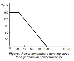
The maximum collector power PC allowed for safe operation is specified at 25°C. For ambient temperature above
this value, PC must be decreased and at the extreme temperature at which the transistor may operate, PC is reduced to zero. A typical power-temperature derating curve, supplied in manufacturer’s specification sheet, is indicated in figure below.
The Condition for Thermal Stability
We now obtain the restrictions to be met if thermal runaway is to be avoided. The required condition is that the rate at which heat is released at collector junction must not exceed the rate at which heat can be dissipated ; that is,
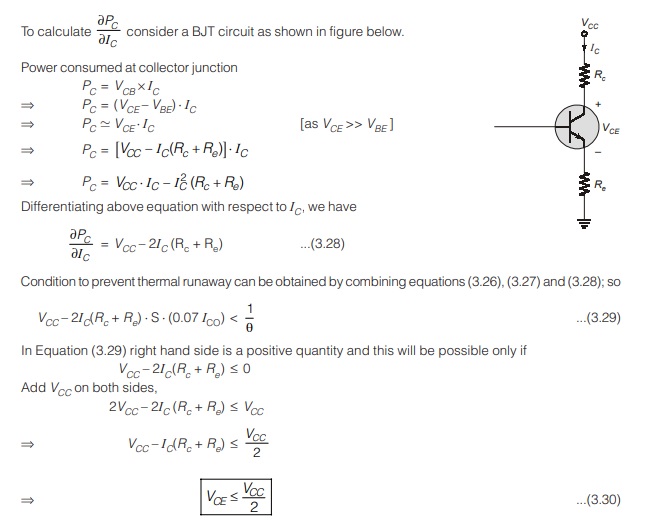
Equation (3.30) gives the condition to avoid thermal runaway.
BJT Biasing in Integrated Circuits (ICs)
Self-bias circuit is preferred to bias BJT in amplifiers which are formed on PCB.
Self bias circuits can not be used to bias BJT in IC amplifiers because R1 are R2 are large resistances and they require greater area of silicon chip.
The chip area required to fabricate a resistor is proportional to the value of resistance.
To fabricate higher resistance large chip area is required ; therefore BJT is biased in IC amplifiers using special circuits known as current mirror.
Constant Current Source (Basic Current Mirror)
A constant current source makes use of the fact that for a transistor in active mode of operation, the collector current is relatively independent of collector voltage. In basic circuit shown in figure below transistors Q1 and Q2 are matched as the circuit is fabricated using IC technology. It may be noted that bases and emitters of Q1 and Q2 are tied together and thus have the same VBE. In addition, transistor Q1 is connected as a diode by shorting its collector to base.
The input current Iref flows through diode connected transistor Q1 and thus establishes a voltage across Q1. This voltage in turn appears between the base and emitter of Q2. Since Q2 is identical to Q1, the emitter current of Q2 will be equal to emitter current of Q1 which is approximately equal to Iref.
Thus, we can say that as long as Q2 is maintained in active region, its collector current IC2 = IO will be approximately equal to Iref. Since the output current Io is reflection or mirror of the reference current Iref, the circuit is often referred to as current mirror.
This mirror effect is however, valid only for large values of β. To study the effect of β on the operation of the current mirror circuit, we analyze it further.
Analysis
The collector currents IC1 and IC2 for transistors Q1 and Q2 can be approximately expressed as
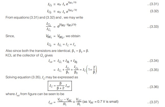
From equation (3.36), for β >> 1, β/(β + 2) is almost unity and the output current IO is equal to the reference current, Iref which for a given R1 is constant. Typical IO varies by about 3% for 50 ≤ β ≤ 200.
Widlar Current Source 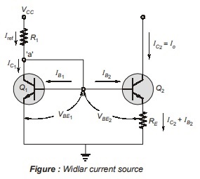
The basic current mirror has a limitation. Whenever, we need low value current source, the value of the resistance R1 required is sufficiently high and can not be fabricated economically in IC circuits. The figure below shows Widlar current source which is particularly suitable for low value of currents. The circuit differs from basic current mirror only in the resistance RE that is included in the emitter lead of Q2. It can be seen that due to RE, the base-emitter voltage VBE2 is less than VBE1 and consequently current Io is smaller than IC1
The ratio of collector currents IC1 and IC2 using equation (3.31) and (3.32) is given by
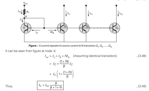
Current Repeaters
The basic current mirror of can be used to source current to more than one load. Such a circuit is called current repeater and is shown in figure below. If all the transistors are identical, then the current IC = IC1⋅⋅⋅ ⋅⋅⋅ = ICN ≅ Iref.
Note:
It is possible to achieve different values of IC1, IC2,….ICN by scaling the emitter area of transistor Q1, Q2, … … QN. The same can also be achieved by using emitter resistance as in the Widlar current source.
Wilson Current Source
The Wilson current source shown in figure below provides an output current IO, which is nearly equal to Iref and also exhibits a very high output resistance.
Analysis
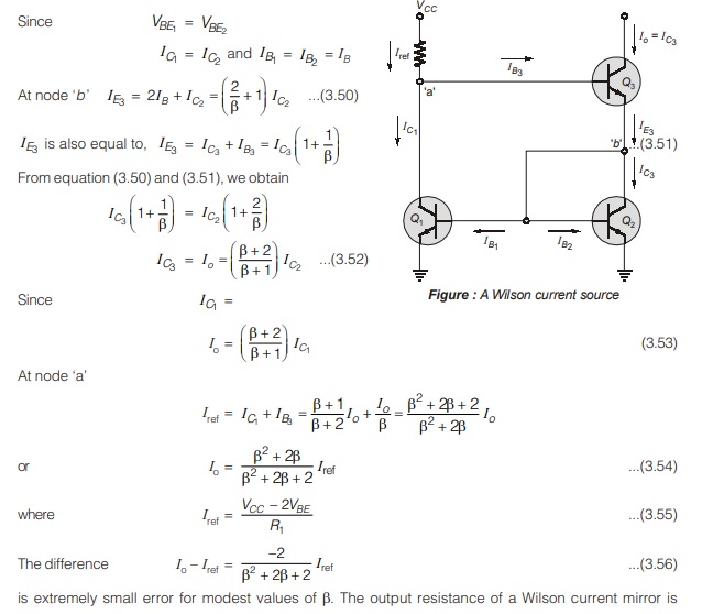
substantially greater ![]() than simple current mirror or Widlar current mirror.
than simple current mirror or Widlar current mirror.
<< Previous | Next >>
Must Read: What are Analog Circuits?
Dear Aspirants,
Your preparation for GATE, ESE, PSUs, and AE/JE is now smarter than ever — thanks to the MADE EASY YouTube channel.
This is not just a channel, but a complete strategy for success, where you get toppers strategies, PYQ–GTQ discussions, current affairs updates, and important job-related information, all delivered by the country’s best teachers and industry experts.
If you also want to stay one step ahead in the race to success, subscribe to MADE EASY on YouTube and stay connected with us on social media.
MADE EASY — where preparation happens with confidence.
MADE EASY is a well-organized institute, complete in all aspects, and provides quality guidance for both written and personality tests. MADE EASY has produced top-ranked students in ESE, GATE, and various public sector exams. The publishing team regularly writes exam-related blogs based on conversations with the faculty, helping students prepare effectively for their exams.