Amplifier Frequency Response
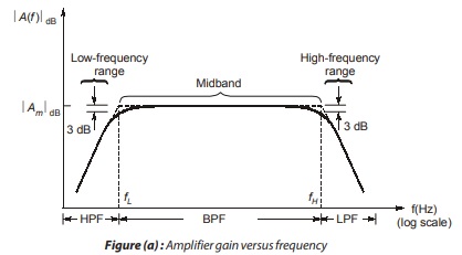
In general, an amplifier gain factor versus frequency will resemble as shown in Figure (a). Both gain factor and frequency are plotted on logarithmic scales (the gain factor in terms of decibels). Three frequency ranges, low, midband and high are indicated. . In low-frequency range, f < fL , the gain decreases with decrease in frequency due to the effect of coupling and bypass capacitor. . In high frequency range, f > fH, stray capacitance and transistor capacitance effect causes the gain to decrease as the frequency increases. The mid-band range is the region where coupling and bypass capacitors act as short-circuit, and stray and transistor is the region where coupling and bypass capacitors act as short-circuit, and stray and transistor capacitances act as open circuit. capacitances act as open circuit. In capacitances act as open circuit. this region, the gain is almost constant. The gain at f = fL and at f = fH is 3-dB less than the maximum midband gain. The bandwidth of the amplifier (in Hz) is defined as
fBW = fH – fL
The Differential Amplifier
The block diagram of differential is shown above. There are two input terminals and one output terminal. Ideally, the output signal is proportional to the difference between two input signals.
The ideal output voltage can be written as
V0 = Avol(V1 – V2)
where Avol is open-loop voltage gain. In ideal case, if V1 = V2, the output voltage is zero. We only obtain a non-zero output voltage if V1 and V2 are not equal.
We define the differential-mode input voltage as
Vd = V1 – V2
and the common-mode input voltage as common-mode input voltage
Vcm = V1 + V2/2
The differential mode voltage for two inputs tells how different they are. The common mode voltage is the part of the voltage that is the same for both i.e. the part they have in common.
The equations show that if V1 = V2, the differential-mode input signal is zero and the common-mode input signal is Vcm = V1 = V2.
If for example, V1 = +10 µV and V2 = –10 µV, then the differential-mode voltage is Vd = 20 µV and the common- mode voltage is Vcm = 0. However, if V1 = 110 µV and V2 = 90 µV, then the differential-mode input signals is 20 µV and Vcm = 100 µV. If each pair of input voltages were applied to ideal differential amplifier, the output voltage in each case would be exactly the same. However, amplifiers are not ideal, and the common-mode input signal does affect the output. The goal of designing differential amplifiers is to minimize the effect of common-mode input signal.
Feedback Amplifiers
An ideal linear amplifier in the mid frequency region provides an output signal that is an exact replica of the applied input signal. But, the practical amplifiers depart from the ideal one for several reasons like non-linearity of transistor characteristics, parameter variation, temperature effects etc. As a matter of fact, some of these factors can be minimized by improving the involved basic device. The best approach is to use the principle of feedback to achieved a desired degree of improvement. The feedback may be defined as a process of injecting some energy from the output and then return it back to the input. Thus, the process of combining a fraction of the output energy (i.e. voltage or current) back to the input is called the feedback. The amplifiers, which use the feedback principle, are known as feedback amplifiers.
Feedback can either be negative or positive. In negative feedback, a portion of output signal is subtracted , from input signal; in positive feedback, a portion of output signal is added to input signal. Negative feedback, for example, tends to maintain a constant value of amplifier voltage gain against variations in transistor parameters, supply voltages, and temperature. Positive feedback is used in the design of oscillators and in number of other applications. In this chapter, we will concentrate on negative feedback.
Types of feedback
Table summarizes the ideal relationships, including the transfer functions, input and output resistances, obtained in the analysis of the four types of feedback amplifier.
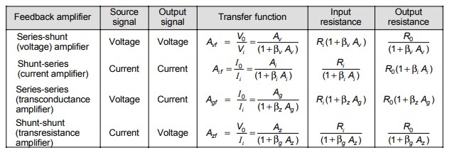
Procedure to identify the type of feedback:
- Step-1: Identify the element responsible for the feedback.
- Step-2: If feedback element is directly connected to the output node, it indicates voltage sampling otherwise it indicates current sampling.
- Step-3: If feedback element is directly connected to the input node, it indicates shunt mixing otherwise it indicates series mixing.
Operational Amplifier
Linear integrated circuits are being used in a number of electronic applications such as in fields like audio and radio communication, medical electronics, instrumentation control, etc. An important linear IC is operational amplifier which will be discussed in this chapter.
An operational amplifier is a direct-coupled high-gain amplifier usually consisting of one or more differential amplifiers and usually followed by a level translator and an output stage. 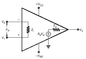
The op-amp can be represented as
Here, V1 is non-inverting terminal voltage
V2 is inverting terminal voltage
Zi is input impedance
Z0 is output impedance
V0 is output voltage
Summing Amplifier
Figure shows the inverting weighted-summer circuit. From our previous discussion, the ideal op-amp will have a virtual ground appearing at its negative input terminal. Ohm’s law tells us that currents i1, i2,….., in are given by
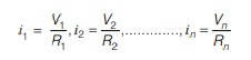
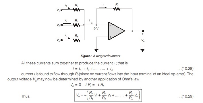
That is, the output voltage is weighted sum of input voltages V1, V2,………., Vn. This circuit is therefore called weighted summer weighted summer. Note that each summing coefficient may be independently adjusted by adjusting the corresponding “feed-in” resistor (R1 to Rn).
<< Previous | Next >>
Must Read: What are Analog Circuits?
Dear Aspirants,
Your preparation for GATE, ESE, PSUs, and AE/JE is now smarter than ever — thanks to the MADE EASY YouTube channel.
This is not just a channel, but a complete strategy for success, where you get toppers strategies, PYQ–GTQ discussions, current affairs updates, and important job-related information, all delivered by the country’s best teachers and industry experts.
If you also want to stay one step ahead in the race to success, subscribe to MADE EASY on YouTube and stay connected with us on social media.
MADE EASY — where preparation happens with confidence.
MADE EASY is a well-organized institute, complete in all aspects, and provides quality guidance for both written and personality tests. MADE EASY has produced top-ranked students in ESE, GATE, and various public sector exams. The publishing team regularly writes exam-related blogs based on conversations with the faculty, helping students prepare effectively for their exams.